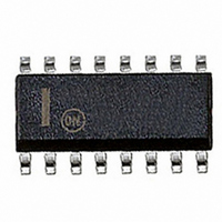
MC74LVX4051DG ON Semiconductor, MC74LVX4051DG Datasheet - Page 11

MC74LVX4051DG
Manufacturer Part Number
MC74LVX4051DG
Description
IC MUX/DEMUX 8X1 16SOIC
Manufacturer
ON Semiconductor
Series
74LVXr
Datasheet
1.MC74LVX4051DTR2G.pdf
(14 pages)
Specifications of MC74LVX4051DG
Function
Multiplexer/Demultiplexer
Circuit
1 x 8:1
On-state Resistance
55 Ohm
Voltage Supply Source
Single Supply
Voltage - Supply, Single/dual (±)
2.5 V ~ 6 V
Current - Supply
40µA
Operating Temperature
-55°C ~ 125°C
Mounting Type
Surface Mount
Package / Case
16-SOIC (0.154", 3.90mm Width)
Lead Free Status / RoHS Status
Lead free / RoHS Compliant
Available stocks
Company
Part Number
Manufacturer
Quantity
Price
Part Number:
MC74LVX4051DG
Manufacturer:
ON/安森美
Quantity:
20 000
V
high and GND being recognized as a logic low. In this
example:
supply voltages V
voltage should not exceed V
analog voltage should not go below V
the difference between V
using the configuration of Figure 21, a maximum analog
signal of five volts peak−to−peak can be controlled. Unused
analog inputs/outputs may be left floating (i.e., not
connected). However, tying unused analog inputs and
)3.0 V
*3.0 V
CC
The Channel Select and Enable control pins should be at
The maximum analog voltage swing is determined by the
or GND logic levels. V
*3.0 V
Figure 20. Application Example
V
ANALOG
SIGNAL
GND = 0 V = logic low
CC
CC
= )5 V = logic high
and V
CC
6
7
8
and V
CC
CC
EE
ON
Figure 22. External Germanium or Schottky Clipping Diodes
. Similarly, the negative peak
. The positive peak analog
being recognized as a logic
16
10
EE
11
9
is five volts. Therefore,
ANALOG
SIGNAL
EE
)3.0 V
. In this example,
TO EXTERNAL CMOS
CIRCUITRY 0 to 3.0 V
DIGITAL SIGNALS
APPLICATIONS INFORMATION
V
V
V
D
D
EE
CC
EE
x
x
http://onsemi.com
MC74LVX4051
)3.0 V
*3.0 V
7
8
ON/OFF
11
outputs to V
minimize crosstalk and feedthrough noise that may be
picked up by an unused switch.
requirement. The only constraints on the power supplies are
that:
anticipated on the analog channels, external Germanium or
Schottky diodes (D
Figure 22. These diodes should be able to absorb the
maximum anticipated current surges during clipping.
V
16
)5 V
CC
GND
Although used here, balanced supplies are not a
When voltage transients above V
V
V
D
D
CC
EE
x
x
Figure 21. Application Example
CC
ANALOG
SIGNAL
V
V
or GND through a low value resistor helps
V
EE
CC
CC
− GND = 0 to *6 volts
− GND = 2.5 to 6 volts
and V
− V
x
) are recommended as shown in
6
7
8
EE
ON
EE
= 2.5 to 6 volts
16
10
v GND
11
9
ANALOG
SIGNAL
CC
)5 V
TO EXTERNAL CMOS
CIRCUITRY 0 to 5 V
DIGITAL SIGNALS
and/or below V
)5 V
GND
EE
are


