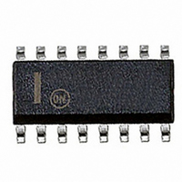
MC74VHC4051DR2G ON Semiconductor, MC74VHC4051DR2G Datasheet

MC74VHC4051DR2G
Specifications of MC74VHC4051DR2G
Available stocks
Related parts for MC74VHC4051DR2G
MC74VHC4051DR2G Summary of contents
Page 1
... These devices are available in Pb- -free package(s). Specifications herein apply to both standard and Pb- -free devices. Please see our website at www.onsemi.com for specific Pb- -free orderable part numbers, or contact your local ON Semiconductor sales office or representative. © Semiconductor Components Industries, LLC, 2006 March, 2006 - - Rev ...
Page 2
ANALOG 12 MULTIPLEXER/ X3 INPUTS/ 1 DEMULTIPLEXER OUTPUTS CHANNEL 10 B SELECT 9 INPUTS C 6 ENABLE PIN PIN 7 = ...
Page 3
Enable V EE Figure 2. Pinout: MC74VHC4051 (Top View ...
Page 4
MAXIMUM RATINGS* Symbol Parameter V Positive DC Supply Voltage CC V Negative DC Supply Voltage (Referenced to GND Analog Input Voltage IS V Digital Input Voltage (Referenced to GND Current, Into or Out of Any ...
Page 5
DC CHARACTERISTICS — Digital Section Symbol Parameter V Minimum High--Level Input IH Voltage, Channel--Select or Enable Inputs V Maximum Low--Level Input IL Voltage, Channel--Select or Enable Inputs I Maximum Input Leakage Current, in Channel--Select or Enable Inputs I Maximum Quiescent ...
Page 6
AC CHARACTERISTICS ( pF, Input t L Symbol Parameter t , Maximum Propagation Delay, Channel--Select to Analog Output PLH t (Figures 18, 19) PHL t , Maximum Propagation Delay, Analog Input to Analog Output PLH t (Figures 20, ...
Page 7
ADDITIONAL APPLICATION CHARACTERISTICS Symbol Parameter BW Maximum On--Channel Bandwidth or Minimum Frequency Response (Figure 15) — Off--Channel Feedthrough Isolation (Figure 16) — Feedthrough Noise. Channel--Select Input to Common I/O (Figure 17) — Crosstalk Between Any Two Switches (Figure 24) (Test ...
Page 8
V , INPUT VOLTAGE (VOLTS), REFERENCED Figure 7. Typical On Resistance --4.5 ...
Page 9
OFF OFF Figure 12. Maximum Off Channel Leakage Current, Any One Channel, Test Set- - OFF V ...
Page 10
CHANNEL 50% SELECT t PLH ANALOG 50% OUT Figure 18. Propagation Delays, Channel Select to Analog Out ANALOG 50 PLH ANALOG 50% OUT Figure 20. Propagation Delays, Analog In to Analog Out ENABLE t ...
Page 11
0.1μF OFF *Includes all probe and jig capacitance Figure 24. Crosstalk Between Any Two Switches, Test Set- - 0.1μF f ...
Page 12
ANALOG ANALOG ON SIGNAL SIGNAL -- --5V Figure 28. Application Example +5V 16 +5V ANALOG ANALOG ON/OFF SIGNAL SIGNAL ...
Page 13
LEVEL A SHIFTER 9 LEVEL B SHIFTER 6 LEVEL ENABLE SHIFTER Figure 33. Function Diagram, VHC4052 11 LEVEL A SHIFTER 10 LEVEL B SHIFTER 9 LEVEL C SHIFTER 6 LEVEL ENABLE SHIFTER Figure 32. Function Diagram, VHC4053 http://onsemi.com 13 ...
Page 14
ORDERING & SHIPPING INFORMATION Device MC74VHC4051D MC74VHC4051DR2 MC74VHC4051DT MC74VHC4051DTR2 MC74VHC4052D MC74VHC4052DR2 MC74VHC4052DT MC74VHC4052DTR2 MC74VHC4053D MC74VHC4053DR2 MC74VHC4053DT MC74VHC4053DTR2 Package SOIC--16 SOIC--16 TSSOP--16 TSSOP--16 SOIC--16 SOIC--16 TSSOP--16 TSSOP--16 SOIC--16 SOIC--16 TSSOP--16 TSSOP--16 http://onsemi.com 14 Shipping 48 Units / Rail 2500 Units / ...
Page 15
-T- - SEATING PLANE 0.25 (0.010 PACKAGE DIMENSIONS D SUFFIX SOIC CASE 751B- -05 ISSUE 0.25 (0.010) ...
Page 16
... DETAIL E H DETAIL American Technical Support: 800--282--9855 Toll Free USA/Canada Japan: ON Semiconductor, Japan Customer Focus Center 2--9--1 Kamimeguro, Meguro--ku, Tokyo, Japan 153--0051 Phone: 81--3--5773--3850 http://onsemi.com NOTES: 1. DIMENSIONING AND TOLERANCING PER ANSI Y14.5M, 1982. 2. CONTROLLING DIMENSION: MILLIMETER. ...


