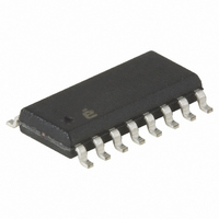
HI9P0201HS-5 Intersil, HI9P0201HS-5 Datasheet - Page 7

HI9P0201HS-5
Manufacturer Part Number
HI9P0201HS-5
Description
IC SWITCH QUAD SPST 16SOIC
Manufacturer
Intersil
Datasheet
1.HI3-0201HS-5.pdf
(11 pages)
Specifications of HI9P0201HS-5
Function
Switch
Circuit
4 x SPST - NC
On-state Resistance
80 Ohm
Voltage Supply Source
Dual Supply
Voltage - Supply, Single/dual (±)
±14 V ~ 16 V
Current - Supply
0.5mA
Operating Temperature
0°C ~ 75°C
Mounting Type
Surface Mount
Package / Case
16-SOIC (0.300", 7.50mm Width)
Lead Free Status / RoHS Status
Contains lead / RoHS non-compliant
Available stocks
Company
Part Number
Manufacturer
Quantity
Price
Company:
Part Number:
HI9P0201HS-5Z
Manufacturer:
Intersil
Quantity:
288
Test Circuits and Waveforms
Application Information
Logic Compatibility
The HI-201HS is TTL compatible. Its logic inputs (pins 1, 8,
9, and 16) are designed to react to digital inputs which
exceed a fixed, internally generated TTL switching threshold.
The HI-201HS can also be driven with CMOS logic (0V-15V),
although the switch performance with CMOS logic will be
inferior to that with TTL logic (0V-5V).
The logic input design of the HI-201HS is largely responsible
for its fast switching speed. It is a design which features a
unique input stage consisting of complementary vertical
PNP and NPN bipolar transistors. This design differs from
that of the standard HI-201 product where the logic inputs
are MOS transistors.
Although the new logic design enhances the switching speed
performance, it also increases the logic input leakage
currents. Therefore, the HI-201HS will exhibit larger digital
input leakage currents in comparison to the standard HI-201
product.
Charge Injection
Charge injection is the charge transferred, through the
internal gate-to-channel capacitances, from the digital logic
input to the analog output. To optimize charge injection
performance for the HI-201HS, it is advisable to provide a
TTL logic input with fast rise and fall times.
If the power supplies are reduced from ±15V, charge
injection will become increasingly dependent upon the digital
input frequency. Increased logic input frequency will result in
larger output error due to charge injection.
-5
0
t
O
FIGURE 2E. V
FIGURE 2. SWITCHING WAVEFORMS FOR VARIOUS ANALOG INPUT VOLTAGES
7
IN
= -5V
(Continued)
HI-201HS
Power Supply Considerations
The electrical characteristics specified in this data sheet are
guaranteed for power supplies V
voltages less than ±15V will result in reduced switch
performance. The following information is intended as a
design aid only.
Single Supply
The switch operation of the HI-201HS is dependent upon an
internally generated switching threshold voltage optimized
for ±15V power supplies. The HI-201HS does not provide the
necessary internal switching threshold in a single supply
system. Therefore, if single supply operation is required, the
HI-300 series of switches is recommended. The HI-300
series will remain operational to a minimum +5V single
supply.
Switch performance will degrade as power supply voltage is
reduced from optimum levels (±15V). So it is recommended
that a single supply design be thoroughly evaluated to
ensure that the switch will meet the requirements of the
application.
For further information see Application Notes AN520,
AN521, AN531, AN532, AN543 and AN557.
-10
POWER SUPPLY
-5
±12 ≤ V
0
VOLTAGES
V
V
V
S
S
S
< ±12V
< ±10V
> ±16V
S
≤ ±15V
t
O
FIGURE 2F. V
Minimal Variation
Parametric variation becomes increasingly
large (increased ON resistance, longer
switching times).
Not Recommended.
Not Recommended.
SWITCH PERFORMANCE
S
IN
= ±15V. Power supply
= -10V


