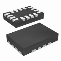
ISL54056IRUZ-T Intersil, ISL54056IRUZ-T Datasheet - Page 9

ISL54056IRUZ-T
Manufacturer Part Number
ISL54056IRUZ-T
Description
IC SWITCH QUAD SPDT 16UTQFN
Manufacturer
Intersil
Datasheet
1.ISL54056IRUZ-T.pdf
(12 pages)
Specifications of ISL54056IRUZ-T
Function
Switch
Circuit
4 x SPDT
On-state Resistance
550 mOhm
Voltage Supply Source
Single Supply
Voltage - Supply, Single/dual (±)
1.65 V ~ 4.5 V
Current - Supply
0.15µA
Operating Temperature
-40°C ~ 85°C
Mounting Type
Surface Mount
Package / Case
16-UTQFN (16-µTQFN)
Lead Free Status / RoHS Status
Lead free / RoHS Compliant
High-Frequency Performance
In 50Ω systems, the ISL54056 has a -3dB bandwidth of
104MHz (see Figure 22). The frequency response is very
consistent over a wide V+ range, and for varying analog
signal levels.
An OFF switch acts like a capacitor and passes higher
frequencies with less attenuation, resulting in signal
feedthrough from a switch’s input to its output. Off isolation is
the resistance to this feedthrough, while crosstalk indicates
the amount of feedthrough from one switch to another.
Figure 23 details the high off isolation and crosstalk rejection
provided by this part. At 100kHz, off isolation is about 65dB
in 50Ω systems, decreasing approximately 20dB per decade
as frequency increases. Higher load impedances decrease
off isolation and crosstalk rejection due to the voltage divider
action of the switch OFF impedance and the load
impedance.
Typical Performance Curves
FIGURE 10. ON-RESISTANCE vs SUPPLY VOLTAGE vs
FIGURE 12. ON-RESISTANCE vs SUPPLY VOLTAGE vs
0.40
0.39
0.38
0.37
0.36
0.35
0.34
0.33
0.32
0.8
0.7
0.6
0.5
0.4
0
0
SWITCH VOLTAGE
SWITCH VOLTAGE
1
0.5
V+ = 1.65V
V+ = 3.9V
V+ = 1.8V
V+ = 4.3V
V+ = 2V
2
V
V
COM
9
COM
1.0
(V)
(V)
V+ = 4.5V
3
T
A
1.5
= +25°C, unless otherwise specified
I
I
COM
COM
4
= 100mA
= 100mA
2.0
5
ISL54056
Leakage Considerations
Reverse ESD protection diodes are internally connected
between each analog-signal pin and both V+ and GND. One of
these diodes conducts if any analog signal exceeds V+ or
GND.
Virtually all the analog leakage current comes from the ESD
diodes to V+ or GND. Although the ESD diodes on a given
signal pin are identical and therefore fairly well balanced,
they are reverse biased differently. Each is biased by either
V+ or GND and the analog signal. This means their leakages
will vary as the signal varies. The difference in the two diode
leakages to the V+ and GND pins constitutes the analog signal
path leakage current. All analog leakage current flows between
each pin and one of the supply terminals, not to the other
switch terminal. This is why both sides of a given switch can
show leakage currents of the same or opposite polarity.
There is no connection between the analog signal paths and
V+ or GND.
FIGURE 11. ON-RESISTANCE vs SUPPLY VOLTAGE vs
0.46
0.45
0.44
0.43
0.42
0.41
0.40
0.39
0.38
0.37
0.36
FIGURE 13. ON-RESISTANCE vs SWITCH VOLTAGE
0.45
0.40
0.35
0.30
0.25
0
0
SWITCH VOLTAGE
0.5
1
1.0
V+ = 2.7V
V+ = 3V
V+ = 3.3V
1.5
2
V
V
-40°C
+85°C
+25°C
COM
COM
(V)
(V)
2.0
3
2.5
I
I
COM
COM
4
August 15, 2007
3.0
V+ = 4.3V
= 100mA
= 100mA
FN6357.4
3.5
5


