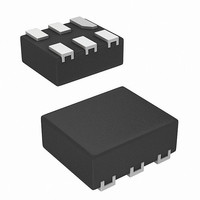
ISL54053IRUZ-T Intersil, ISL54053IRUZ-T Datasheet

ISL54053IRUZ-T
Specifications of ISL54053IRUZ-T
Related parts for ISL54053IRUZ-T
ISL54053IRUZ-T Summary of contents
Page 1
... CAUTION: These devices are sensitive to electrostatic discharge; follow proper IC Handling Procedures. | 1-888-INTERSIL or 1-888-468-3774 Intersil (and design registered trademark of Intersil Americas Inc. Copyright © Intersil Americas Inc. 2007, 2009. All Rights Reserved All other trademarks mentioned are the property of their respective owners. ...
Page 2
... Ordering Information PART NUMBER PART (Notes 1, 4) MARKING ISL54053IRUZ-T(Note 2) C ISL54053IHZ-T (Note 3) 4053 NOTES: 1. Please refer to TB347 for details on reel specifications. 2. These Intersil Pb-free plastic packaged products employ special Pb-free material sets; molding compounds/die attach materials and NiPdAu plate - e4 termination finish, which is RoHS compliant and compatible with both SnPb and Pb-free soldering operations ...
Page 3
... Ld SOT-23 (Notes Maximum Junction Temperature (Plastic Package). . Maximum Storage Temperature Range -65°C to +150°C Pb-Free Reflow Profile . . . . . . . . . . . . . . . . . .see link below http://www.intersil.com/pbfree/Pb-FreeReflow.asp Operating Conditions V+ (Positive DC Supply Voltage 1.8V to 5.5V Analog Signal Range . . . . . . . . . . . . . . . . . . . . . . (Digital Logic Input Voltage (IN) ...
Page 4
Electrical Specifications - 5V Supply PARAMETER Total Harmonic Distortion f = 20Hz to 20kHz 600Ω L -3dB Bandwidth R = 50Ω OFF Capacitance 4.5V 1MHz (See Figure ...
Page 5
Electrical Specifications - 3V Supply PARAMETER COM ON Capacitance 1MHz (See Figure 7) COM(ON) DIGITAL INPUT CHARACTERISTICS Input Voltage Low, V INL Input Voltage High, V INH Input Current 3.6V, V ...
Page 6
Test Circuits and Waveforms V INH LOGIC 50% INPUT V INL t OFF SWITCH V Nx INPUT V 90% SWITCH OUTPUT Logic input waveform is inverted for switches that have the opposite logic sense. FIGURE 1A. MEASUREMENT ...
Page 7
Test Circuits and Waveforms SIGNAL GENERATOR COM ANALYZER GND R L FIGURE 4. OFF ISOLATION TEST CIRCUIT 50Ω ANALYZER GND R L FIGURE 6. CROSSTALK TEST ...
Page 8
OPTIONAL SCHOTTKY DIODE V+ OPTIONAL PROTECTION RESISTOR GND OPTIONAL SCHOTTKY DIODE FIGURE 8. OVERVOLTAGE PROTECTION Power-Supply Considerations The ISL54053 construction is typical of most single supply CMOS analog switches, in that they have two supply pins: ...
Page 9
Typical Performance Curves 2.5 2 1.8V 1 2. (V) COM FIGURE 9. ON-RESISTANCE vs SUPPLY VOLTAGE vs SWITCH VOLTAGE 1.5 1.4 1.3 1.2 ...
Page 10
Typical Performance Curves 1.6 1.4 1.2 V INH 1.0 0.8 0.6 0.4 0.2 2.0 2.5 3.0 3.5 4.0 V+ (V) FIGURE 15. DIGITAL SWITCHING POINT vs SUPPLY VOLTAGE 1.8V to 5.5V -20 -40 ISOLATION CROSSTALK -60 -80 ...
Page 11
... The pin #1 identifier may be either a mold or mark feature. 7. Maximum package warpage is 0.05mm. 8. Maximum allowable burrs is 0.076mm in all directions. 9. JEDEC Reference MO-255. 10. For additional information, to assist with the PCB Land Pattern Design effort, see Intersil Technical Brief TB389. 0.35 10 MILLIMETERS MIN NOMINAL MAX 0 ...
Page 12
... Accordingly, the reader is cautioned to verify that data sheets are current before placing orders. Information furnished by Intersil is believed to be accurate and reliable. However, no responsibility is assumed by Intersil or its subsidiaries for its use; nor for any infringements of patents or other rights of third parties which may result from its use. No license is granted by implication or otherwise under any patent or patent rights of Intersil or its subsidiaries ...


