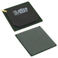
LFE3-35EA-8FN672I Lattice, LFE3-35EA-8FN672I Datasheet - Page 2

LFE3-35EA-8FN672I
Manufacturer Part Number
LFE3-35EA-8FN672I
Description
IC FPGA 33.3K LUTS 310I/O FN672
Manufacturer
Lattice
Series
ECP3r
Datasheets
1.LFE3-150EA-7FN672C.pdf
(136 pages)
2.LFE3-35EA-8FN672I.pdf
(4 pages)
3.LFE3-35EA-8FN672I.pdf
(21 pages)
Specifications of LFE3-35EA-8FN672I
Number Of Logic Elements/cells
33000
Number Of Labs/clbs
4125
Total Ram Bits
1358848
Number Of I /o
310
Number Of Gates
-
Voltage - Supply
1.14 V ~ 1.26 V
Mounting Type
Surface Mount
Operating Temperature
-40°C ~ 100°C
Package / Case
672-BBGA
Lead Free Status / Rohs Status
Lead free / RoHS Compliant
Other names
220-1163
LatticeECP3 Architecture
Architecture Overview
LatticeECP3 FPGAs utilize Lattice’ s third
generation of cost optimized transceiv-
ers and a low-power 65-nm process
FPGA architecture. Building on the
successful LatticeECP2M™ FPGA fam-
ily, LatticeECP3 devices deliver high-
performance SERDES blocks, cascadable
high-performance sysDSP™, ultra-high
logic and sysMEM™ embedded RAM,
distributed memory, sysCLOCK PLLs,
DDR3 memory interface, and sysIO buf-
fers. LatticeECP3 provides a low-cost,
low-power programmable solution for
a wide variety of wireless and wireline
applications.
sysDSP BLOCK DIAGRAM
PROGRAMMABLE FUNCTION UNIT
(PFU) BLOCK DIAGRAM
Routing
From
Output Registers
Input Registers
∑ ± & + ⊕
==
Multipliers
Registers
Slice 0
Pipeline
ALU
Carry Chain
LUT4
LUT4
LUT4
LUT4
LUT4
LUT4
LUT4
LUT4
Carry Chain
Slice 3
Slice 2
Slice 1
Slice 0
Output Registers
Input Registers
∑ ± & + ⊕
FF
FF
FF
FF
FF
FF
Slice 1
==
Multipliers
Registers
Pipeline
ALU
Routing
To
LatticeECP3 BLOCK DIAGRAM
sysMEM CONFIG OPTIONS
sysCLOCK PLL BLOCK DIAGRAM
LatticeECP3 EBR SRAM (Mbits)
Feedback
sysCLOCK PLLs
& DLLs for clock
management.
Flexible sysIO
Buffers support
LVCMOS, HSTL,
SSTL, LVDS and
more.
Control
Signals
Clock
Reset
Input
Clock
Programmable
Function Unit
(PFU)
perform Logic,
Arithmetic,
Distributed RAM
and Distributed
ROM functions.
Single Port
7
6
5
4
3
2
1
0
On-Chip
Oscillator
16384 x 1
1024 x 18
8192 x 2
4096 x 4
2048 x 9
512 x 36
17K
Internal Feedback
7Mb
UP TO
Frequency
Detector /
Oscillator
33K
Voltage
Control
Configuration Logic supports dual boot,
encryption and TransFR updates.
Phase
Dual Port
16384 x 1
1024 x 18
8192 x 2
4096 x 4
2048 x 9
LUTs
—
67K
Duty Cycle/
Duty Trim
Duty Trim
Phase/
Divider
Lock Detect
92K
Pseudo-Dual
SERDES
16384 x 1
1024 x 18
8192 x 2
4096 x 4
2048 x 9
512 x 36
Port
÷3
149K
SERDES
SERDES
Fabric
Sector 0
Sector 1
PRE-ENGINEERED SOURCE
SYNCHRONOUS INTERFACES
DUAL-BOOT AND 128-BIT AES
ENCRYPTION
FPGA
Embedded 3.2Gbps SERDES support PCI
Express, Ethernet (XAUI, 1GbE, SGMII),
CPRI, and 3G/HD/SD-SDI.
sysMEM Embedded Block RAM (EBR)
provides 18kbit dual port RAM.
DDR3 (800 Mbps)
7:1 LVDS, ADC/DAC
SPI Configuration
[
[
SERDES
Configuration A
Configuration B
Gearbox
Gearbox
Memory
4:1
4:1
DQS/Strobe Delay & Transition Detect
& Write Clock Generation
Output Register
Register Block
(15 Flip/Flops)
Input Register
(2 Flip/Flops)
(6 Flip/Flops)
Control
Tri-State
Read
Data
Block
Block
Pre-Engineered
Source Synchronous
Support implements
DDR3 at 800Mbps
and generic
interfaces up to
1Gbps.
128-bit Key
Cascadable sysDSP
Blocks implements
high-performance
multiplier, MAC,
wide adder trees,
and ALU functions
efficiently.
Decryption
JTAG
LatticeECP3
Engine
Correction
ISI
FPGA
Logic


