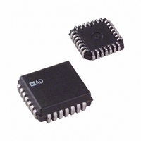
ADG407BP Analog Devices Inc, ADG407BP Datasheet - Page 16

ADG407BP
Manufacturer Part Number
ADG407BP
Description
IC MULTIPLEXER DUAL 8X1 28PLCC
Manufacturer
Analog Devices Inc
Series
LC²MOSr
Type
Analog Multiplexerr
Datasheet
1.ADG406BNZ.pdf
(20 pages)
Specifications of ADG407BP
Mounting Type
Surface Mount
Package / Case
28-LCC (J-Lead)
Rohs Status
RoHS non-compliant
Function
Multiplexer
Circuit
2 x 8:1
On-state Resistance
80 Ohm
Voltage Supply Source
Single Supply
Voltage - Supply, Single/dual (±)
5V, 12V
Current - Supply
100µA
Operating Temperature
-40°C ~ 85°C
Peak Reflow Compatible (260 C)
No
No. Of Circuits
8
Leaded Process Compatible
No
No. Of Channels
8
Analog Multiplexer Type
Differential
Multiplexer Configuration
Dual 8:1
Number Of Inputs
16
Number Of Outputs
2
Number Of Channels
2
Analog Switch On Resistance
125@10.8VOhm
Analog Switch Turn On Time
240ns
Analog Switch Turn Off Time
180ns
Package Type
PLCC
Power Supply Requirement
Single/Dual
Single Supply Voltage (typ)
12V
Single Supply Voltage (max)
25V
Dual Supply Voltage (typ)
±15V
Dual Supply Voltage (max)
±22V
Supply Current
0.2@±16.5VmA
Mounting
Surface Mount
Pin Count
28
Operating Temp Range
-40C to 85C
Operating Temperature Classification
Industrial
Lead Free Status / Rohs Status
Not Compliant
Available stocks
Company
Part Number
Manufacturer
Quantity
Price
Company:
Part Number:
ADG407BP
Manufacturer:
AD
Quantity:
5 510
Company:
Part Number:
ADG407BP
Manufacturer:
AD
Quantity:
5 510
Company:
Part Number:
ADG407BP-REEL
Manufacturer:
Analog Devices Inc
Quantity:
10 000
Company:
Part Number:
ADG407BPZ
Manufacturer:
Analog Devices Inc
Quantity:
10 000
Part Number:
ADG407BPZ
Manufacturer:
ADI/亚德诺
Quantity:
20 000
ADG406/ADG407/ADG426
1
2.4V
SIMILAR CONNECTION FOR ADG406/ADG407
2.4V
V
IN
V
RS
V
IN
V
2.4V
WR
50Ω
A3
A2
A1
A0
EN
RS
A3
A2
A1
A0
EN
RS
WR
V
V
V
V
DD
DD
GND
DD
DD
ADG426
ADG426
S2 THRU S16
S2 THRU S16
GND
A3
A2
A1
A0
RS
EN
WR
V
V
GND
V
V
V
V
DD
DD
SS
SS
ADG426
SS
SS
S2 THRU S16
S1
S1
D
D
WR
V
V
SS
SS
1
R
300Ω
R
300Ω
S1
D
L
L
V
V
S
S
Figure 31. Enable Delay, t
Figure 32. Write Turn-On Time, t
Figure 33. Reset Turn-Off Time, t
C
35pF
C
35pF
R
300Ω
L
L
L
V
V
V
S
OUT
OUT
Rev. B | Page 16 of 20
C
35pF
OUTPUT
L
RS
V
OUTPUT
OUT
3V
0V
0V
V
0
WR
3V
0V
0V
V
DRIVE (V
0
ON
ENABLE
OUTPUT
(EN), t
V
3V
0V
0V
IN
O
ON
OFF
)
OFF
(WR)
(RS)
(EN)
50%
t
ON
50%
50%
(EN)
t
OFF
90%
t
(RS)
ON
(WR)
50%
0.8V
90%
0.2V
0
t
OFF
0
(EN)


