ADG529AKP Analog Devices Inc, ADG529AKP Datasheet - Page 10
ADG529AKP
Manufacturer Part Number
ADG529AKP
Description
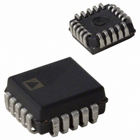
IC MULTIPLEXER DUAL 4X1 20PLCC
Manufacturer
Analog Devices Inc
Type
Analog Multiplexerr
Datasheet
1.ADG529AKNZ.pdf
(12 pages)
Specifications of ADG529AKP
Rohs Status
RoHS non-compliant
Function
Multiplexer
Circuit
2 x 4:1
On-state Resistance
300 Ohm
Voltage Supply Source
Dual Supply
Voltage - Supply, Single/dual (±)
±10.8 V ~ 16.5 V
Current - Supply
20µA
Operating Temperature
-40°C ~ 85°C
Mounting Type
Surface Mount
Package / Case
20-LCC (J-Lead)
Package
20PLCC
Maximum On Resistance
700@16.5V Ohm
Maximum Propagation Delay Bus To Bus
300@±16.5V|450@16.5V ns
Maximum High Level Output Current
20 mA
Multiplexer Architecture
4:1
Maximum Turn-on Time
450@16.5V ns
Power Supply Type
Single|Dual
Available stocks
Company
Part Number
Manufacturer
Quantity
Price
Company:

Part Number:
ADG529AKP
Manufacturer:
Analog Devices Inc
Quantity:
10 000
Company:
Part Number:
ADG529AKPZ
Manufacturer:
NXP
Quantity:
10 148
Company:
Part Number:
ADG529AKPZ
Manufacturer:
Analog Devices Inc
Quantity:
10 000


ADG528A/ADG529A
TERMINOLOGY
R
R
R
I
I
I
V
C
C
C
t
S
D
D
ON
S
ON
ON
ON
S
D
IN
(OFF)
(OFF)
(ON)
(V
(OFF)
(OFF)
(EN)
Match Difference between the RON of any two channels
Drift
D
)
Ohmic resistance between terminals D and S
Change in RON versus temperature
Source terminal leakage current when the switch
is off.
Drain terminal leakage current when the switch is
off.
Leakage current that flows from the closed switch
into the body.
Analog voltage on terminal S or D
Channel input capacitance for “OFF” condition
Channel output capacitance for “OFF” condition
Digital input capacitance
Delay time between the 50% and 90% points of
the digital input and switch “ON” condition.
0.048 (1.21)
0.042 (1.07)
0.020
(0.50)
R
0.180 (4.57)
0.150 (3.81)
0.110 (2.79)
0.048 (1.21)
0.042 (1.07)
4
8
CONTROLLING DIMENSIONS ARE IN INCHES; MILLIMETER DIMENSIONS
(IN PARENTHESES) ARE ROUNDED-OFF INCH EQUIVALENTS FOR
REFERENCE ONLY AND ARE NOT APPROPRIATE FOR USE IN DESIGN
0.395 (10.02)
0.385 (9.78)
CONTROLLING DIMENSIONS ARE IN INCHES; MILLIMETER DIMENSIONS
(IN PARENTHESES) ARE ROUNDED-OFF INCH EQUIVALENTS FOR
REFERENCE ONLY AND ARE NOT APPROPRIATE FOR USE IN DESIGN
0.356 (9.04)
0.350 (8.89) SQ
MAX
3
(PINS DOWN)
9
TOP VIEW
18-Lead Plastic Dual In-Line Package [PDIP]
20-Lead Plastic Leaded Chip Carrier [PLCC]
0.022 (0.558)
0.014 (0.356)
Dimensions shown in inches and (millimeters)
Dimensions shown in inches and (millimeters)
19
13
COMPLIANT TO JEDEC STANDARDS MO-095AD
SQ
COMPLIANT TO JEDEC STANDARDS MO-047AA
18
1
18
14
0.885 (22.48)
0.845 (21.46)
0.056 (1.42)
0.042 (1.07)
OUTLINE DIMENSIONS
0.050
(1.27)
BSC
0.015 (0.38) MIN
0.100
(2.54)
BSC
0.060 (1.52)
0.045 (1.14)
0.180 (4.57)
0.165 (4.19)
(P-20A)
10
(N-18)
0.120 (3.04)
0.090 (2.29)
9
–10–
t
t
t
V
V
I
V
V
I
I
SEATING
PLANE
OFF
TRANSITION
OPEN
INL
DD
SS
0.295 (7.49)
0.275 (6.99)
INL
INH
DD
SS
0.032 (0.81)
0.026 (0.66)
0.021 (0.53)
0.013 (0.33)
0.20 (0.51)
MIN
0.040 (1.01)
0.025 (0.64)
(I
(EN)
INH
0.325 (8.26)
0.300 (7.62)
)
0.330 (8.38)
0.290 (7.37)
0.015 (0.381)
0.008 (0.203)
R
Delay time between the 50% and 10% points of
the digital input and switch “OFF” condition
Delay time between the 50% and 90% points of
the digital inputs and switch “ON” condition
when switching from one address state to another.
“OFF” time measured between 50% points of
both switches when switching from one address
state to another
Maximum input voltage for Logic “0”
Minimum input voltage for Logic “1”
Input current of the digital input
Most positive voltage supply
Most negative voltage supply
Positive supply current
Negative supply current
0.020 (0.50)
0.180 (4.57)
MAX
R
BOTTOM
(PINS UP)
VIEW
REV. B
Related parts for ADG529AKP
Image
Part Number
Description
Manufacturer
Datasheet
Request
R

Part Number:
Description:
±1.7g Dual-Axis IMEMS Accelerometer Evaluation Board
Manufacturer:
Analog Devices Inc
Datasheet:

Part Number:
Description:
Inertial Sensor Evaluation System
Manufacturer:
Analog Devices Inc
Datasheet:
Part Number:
Description:
Manufacturer:
Analog Devices Inc
Datasheet:
Part Number:
Description:
Manufacturer:
Analog Devices Inc
Datasheet:
Part Number:
Description:
Manufacturer:
Analog Devices Inc
Datasheet:
Part Number:
Description:
Manufacturer:
Analog Devices Inc
Datasheet:
Part Number:
Description:
Manufacturer:
Analog Devices Inc
Datasheet:
Part Number:
Description:
Manufacturer:
Analog Devices Inc
Datasheet:
Part Number:
Description:
Manufacturer:
Analog Devices Inc
Datasheet:
Part Number:
Description:
Manufacturer:
Analog Devices Inc
Datasheet:
Part Number:
Description:
Manufacturer:
Analog Devices Inc
Datasheet:
Part Number:
Description:
Manufacturer:
Analog Devices Inc
Datasheet:
Part Number:
Description:
Manufacturer:
Analog Devices Inc
Datasheet: