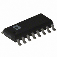
ADG713BR Analog Devices Inc, ADG713BR Datasheet - Page 5

ADG713BR
Manufacturer Part Number
ADG713BR
Description
IC SWITCH QUAD SPST 16SOIC
Manufacturer
Analog Devices Inc
Datasheet
1.ADG711BRUZ.pdf
(12 pages)
Specifications of ADG713BR
Rohs Status
RoHS non-compliant
Function
Switch
Circuit
4 x SPST - NC/NO
On-state Resistance
4 Ohm
Voltage Supply Source
Single Supply
Voltage - Supply, Single/dual (±)
1.8 V ~ 5.5 V
Current - Supply
0.001µA
Operating Temperature
-40°C ~ 85°C
Mounting Type
Surface Mount
Package / Case
16-SOIC (0.154", 3.90mm Width)
Available stocks
Company
Part Number
Manufacturer
Quantity
Price
Part Number:
ADG713BR
Manufacturer:
ADI/亚德诺
Quantity:
20 000
Company:
Part Number:
ADG713BR-REEL7
Manufacturer:
SEMTECH
Quantity:
1 758
Part Number:
ADG713BRU
Manufacturer:
ADI/亚德诺
Quantity:
20 000
Part Number:
ADG713BRU-REEL
Manufacturer:
ADI/亚德诺
Quantity:
20 000
Part Number:
ADG713BRUZ
Manufacturer:
ADI/亚德诺
Quantity:
20 000
Company:
Part Number:
ADG713BRUZ-REEL7
Manufacturer:
Infineon
Quantity:
91
Part Number:
ADG713BRUZ-REEL7
Manufacturer:
ADI/亚德诺
Quantity:
20 000
REV. A
V
GND
S
D
IN
R
∆R
R
I
I
I
V
C
C
C
t
S
D
D
ON
DD
ON
FLAT(ON)
D
S
D
D
, I
(OFF)
(OFF)
ON
, C
(OFF)
(V
(OFF)
S
ADG711 In
0
1
Logic
0
1
S
(ON)
S
)
(ON)
Table I. Truth Table (ADG711/ADG712)
Table II. Truth Table (ADG713)
Most positive power supply potential.
Ground (0 V) reference.
Source terminal. May be an input or output.
Drain terminal. May be an input or output.
Logic control input.
Ohmic resistance between D and S.
On resistance match between any two chan-
nels, i.e., R
Flatness is defined as the difference between
the maximum and minimum value of on
resistance as measured over the specified
analog signal range.
Source leakage current with the switch “OFF.”
Drain leakage current with the switch “OFF.”
Channel leakage current with the switch “ON.”
Analog voltage on terminals D, S.
“OFF” switch source capacitance.
“OFF” switch drain capacitance.
“ON” switch capacitance.
Delay between applying the digital control
input and the output switching on.
ADG712 In
1
0
Switch 1, 4
OFF
ON
ON
max–R
Switch Condition
ON
OFF
Switch 2, 3
ON
OFF
ON
min.
TERMINOLOGY
–5–
t
t
Crosstalk
Off Isolation
Charge
Bandwidth
On Response
On Loss
OFF
Injection
D
Delay between applying the digital control
input and the output switching off.
“OFF” time or “ON” time measured
between the 90% points of both switches,
when switching from one address state to
another. (ADG713 only).
A measure of unwanted signal that is coupled
through from one channel to another as a
result of parasitic capacitance.
A measure of unwanted signal coupling
through an “OFF” switch.
A measure of the glitch impulse transferred
from the digital input to the analog output
during switching.
The frequency at which the output is attenu-
ated by 3 dB.
The frequency response of the “ON” switch.
The voltage drop across the “ON” switch,
seen on the on response vs. frequency plot as
how many dBs the signal is away from
0 dB at very low frequencies.
PIN CONFIGURATION
ADG711/ADG712/ADG713
GND
IN1
IN4
NC
D1
S1
S4
D4
(TSSOP/SOIC)
NC = NO CONNECT
1
2
3
4
5
6
7
8
(Not to Scale)
TOP VIEW
ADG711
ADG712
ADG713
16
15
14
13
12
11
10
9
IN2
D2
S2
V
NC
S3
D3
IN3
DD


