ADG801BRTZ-REEL7 Analog Devices Inc, ADG801BRTZ-REEL7 Datasheet
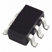
IC SWITCH SPST SOT23-6

ADG801BRTZ-REEL7

Manufacturer Part Number
ADG801BRTZ-REEL7
Description
IC SWITCH SPST SOT23-6
Manufacturer
Analog Devices Inc
Type
Analog Switchr
Datasheet

Specifications of ADG801BRTZ-REEL7

Function
Switch
Circuit
1 x SPST- NO
On-state Resistance
300 mOhm
Voltage Supply Source
Single Supply
Voltage - Supply, Single/dual (±)
1.8 V ~ 5.5 V
Current - Supply
0.001µA
Operating Temperature
-40°C ~ 85°C
Mounting Type
Surface Mount
Package / Case
SOT-23-6
Analog Switch Type
SPST
No. Of Channels
1
Bandwidth
12MHz
On State Resistance Max
0.25ohm
Turn Off Time
9ns
Turn On Time
35ns
Supply Voltage Range
1.8V To 5.5V
Multiplexer Configuration
Single SPST
Number Of Inputs
1
Number Of Outputs
1
Number Of Channels
1
Analog Switch On Resistance
0.6@3.6VOhm
Analog Switch Turn On Time
55ns
Analog Switch Turn Off Time
15ns
Package Type
SOT-23
Power Supply Requirement
Single
Single Supply Voltage (min)
1.8V
Single Supply Voltage (typ)
3/5V
Single Supply Voltage (max)
5.5V
Dual Supply Voltage (min)
Not RequiredV
Dual Supply Voltage (typ)
Not RequiredV
Dual Supply Voltage (max)
Not RequiredV
Supply Current
0.001mA
Mounting
Surface Mount
Pin Count
6
Operating Temp Range
-40C to 125C
Operating Temperature Classification
Automotive
Lead Free Status / RoHS Status
Lead free / RoHS Compliant
Lead Free Status / RoHS Status
Lead free / RoHS Compliant, Lead free / RoHS Compliant

Available stocks

Company
Part Number
Manufacturer
Quantity
Price
Part Number:
ADG801BRTZ-REEL7
Manufacturer:
ADI/亚德诺
Quantity:
20 000
FEATURES
0.4 Ω maximum on resistance @ 125°C
0.08 Ω maximum on resistance flatness @ 125°C
1.8 V to 5.5 V single supply
Automotive temperature range from −40°C to +125°C
400 mA current-carrying capability
Tiny 6-lead SOT-23, 8-lead MSOP, and 6-ball WLCSP packages
35 ns switching times
Low power consumption
TTL-/CMOS-compatible inputs
Pin compatible with ADG701/ADG702
APPLICATIONS
Power routing
Cellular phones
Modems
PCMCIA cards
Hard drives
Data acquisition systems
Communications systems
Relay replacement
Battery-powered systems
GENERAL DESCRIPTION
The ADG801 and ADG802 are monolithic CMOS, single-pole,
single throw (SPST) switches with on resistance of less than
0.4 Ω. These switches are designed using an advanced
submicron process that provides extremely low on resistance,
high switching speed, and low leakage currents.
The low on resistance of <0.4 Ω makes these parts ideal for
applications where low on resistance switching is critical.
The ADG801 switch is normally open (NO), while the ADG802
is normally closed (NC). Each switch conducts equally well in
both directions when on.
Rev. A
Information furnished by Analog Devices is believed to be accurate and reliable. However, no
responsibility is assumed by Analog Devices for its use, nor for any infringements of patents or other
rights of third parties that may result from its use. Specifications subject to change without notice. No
license is granted by implication or otherwise under any patent or patent rights of Analog Devices.
Trademarks and registered trademarks are the property of their respective owners.
One Technology Way, P.O. Box 9106, Norwood, MA 02062-9106, U.S.A.
Tel: 781.329.4700
Fax: 781.461.3113
PRODUCT HIGHLIGHTS
1.
2.
3.
4.
5.
6.
Low on resistance (0.25 Ω typical).
1.8 V to 5.5 V single-supply operation.
Tiny 6-lead SOT-23, 8-lead MSOP, and 6-ball WLCSP
packages.
400 mA current-carrying capability.
Automotive temperature range from −40°C to +125°C.
Pin compatible with ADG701 (ADG801) and ADG702
(ADG802).
<0.4 Ω CMOS 1.8 V to 5.5 V
FUNCTIONAL BLOCK DIAGRAM
©2002–2007 Analog Devices, Inc. All rights reserved.
S
S
SWITCHES SHOWN FOR
A LOGIC 1 INPUT
ADG801
ADG802
ADG801/ADG802
Figure 1.
SPST Switches
IN
IN
D
D
www.analog.com

Related parts for ADG801BRTZ-REEL7

ADG801BRTZ-REEL7 Summary of contents

Page 1

FEATURES 0.4 Ω maximum on resistance @ 125°C 0.08 Ω maximum on resistance flatness @ 125°C 1 5.5 V single supply Automotive temperature range from −40°C to +125°C 400 mA current-carrying capability Tiny 6-lead SOT-23, 8-lead MSOP, and ...

Page 2

ADG801/ADG802 TABLE OF CONTENTS Features .............................................................................................. 1 Applications....................................................................................... 1 Functional Block Diagram .............................................................. 1 General Description ......................................................................... 1 Product Highlights ........................................................................... 1 Revision History ............................................................................... 2 Specifications..................................................................................... 3 Absolute Maximum Ratings............................................................ 5 REVISION HISTORY 3/07—Rev Rev. A Updated ...

Page 3

SPECIFICATIONS ± 10%, GND = 0 V, unless otherwise noted. The automotive temperature range is −40°C to +125°C. DD Table 1. Parameter 25°C ANALOG SWITCH Analog Signal Range On Resistance (R ) 0.25 ON 0.3 On ...

Page 4

ADG801/ADG802 3.6 V, GND = 0 V, unless otherwise noted. The automotive temperature range is −40°C to +125°C. DD Table 2. Parameter 25°C ANALOG SWITCH Analog Signal Range On Resistance (R ) 0.4 ON 0.6 ...

Page 5

ABSOLUTE MAXIMUM RATINGS T = 25°C, unless otherwise noted. A Parameter Rating V to GND −0 Analog Inputs 1 −0 VDD + 0 mA, whichever occurs first 1 Digital Inputs ...

Page 6

ADG801/ADG802 PIN CONFIGURATIONS AND FUNCTION DESCRIPTIONS Table 4. Pin Function Descriptions Pin Number SOT-23 MSOP WLCSP ...

Page 7

TERMINOLOGY V DD The most positive power supply potential Positive supply current. GND Ground (0 V) reference. S The source terminal can be an input or an output. D The drain terminal can be an input or an ...

Page 8

ADG801/ADG802 TYPICAL PERFORMANCE CHARACTERISTICS 0. 2. 3. 3.3V DD 0.35 V 0.30 0.25 0.20 0. 5.0V DD 0.10 0. 1.0 2.0 3 (V) ...

Page 9

T = 25° 3V –20 –30 –40 –50 –60 –70 0.1 1 FREQUENCY (MHz) Figure 11. Off Isolation vs. Frequency 0 –1 –2 –3 –4 –5 –6 – 25°C A –8 V ...

Page 10

ADG801/ADG802 TEST CIRCUITS V1 Figure 14. On Resistance 0.1µ (OFF) (OFF ...

Page 11

V DD 0.1µ 50Ω 50Ω GND OFF ISOLATION = 20 log Figure 19. Off Isolation V DD 0.1µF NETWORK ANALYZER 50Ω 50Ω GND ...

Page 12

ADG801/ADG802 OUTLINE DIMENSIONS INDICATOR 0.15 MAX 2.90 BSC 2.80 BSC 1.60 BSC PIN 1 0.95 BSC 1.90 1.30 BSC 1.15 0.90 1.45 MAX 0.22 0.08 0.50 SEATING 0.30 PLANE COMPLIANT TO JEDEC STANDARDS MO-178-AB ...

Page 13

BALL 1 2.38 IDENTIFIER 2.18 1.98 TOP VIEW (BALL SIDE DOWN) Figure 23. 6-Ball Wafer Level Chip Scale Package [WLCSP] Dimensions shown in millimeters 0.67 0.57 0.47 0.50 SEATING PLANE 0.32 NOM 0.50 BALL ...

Page 14

... ADG801BRT-REEL7 −40°C to +125°C 2 ADG801BRTZ-500RL7 −40°C to +125°C 2 ADG801BRTZ-REEL −40°C to +125°C 2 ADG801BRTZ-REEL7 −40°C to +125°C ADG802BCB-REEL7 −40°C to +125°C 2 ADG802BCBZ-REEL7 −40°C to +125°C ADG802BRM-R2 −40°C to +125°C ADG802BRM −40°C to +125°C ADG802BRM-REEL − ...

Page 15

NOTES Rev Page ADG801/ADG802 ...

Page 16

ADG801/ADG802 NOTES ©2002–2007 Analog Devices, Inc. All rights reserved. Trademarks and registered trademarks are the property of their respective owners. D02800-0-3/07(A) Rev Page ...

Related keywords