ADG849YKSZ-500RL7 Analog Devices Inc, ADG849YKSZ-500RL7 Datasheet - Page 6
ADG849YKSZ-500RL7
Manufacturer Part Number
ADG849YKSZ-500RL7
Description
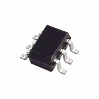
IC SWITCH SPDT SC70-6
Manufacturer
Analog Devices Inc
Type
Analog Switchr
Datasheet
1.ADG849YKSZ-REEL.pdf
(12 pages)
Specifications of ADG849YKSZ-500RL7
Function
Switch
Circuit
1 x SPDT
On-state Resistance
600 mOhm
Voltage Supply Source
Single Supply
Voltage - Supply, Single/dual (±)
5V
Current - Supply
0.001µA
Operating Temperature
-40°C ~ 125°C
Mounting Type
Surface Mount
Package / Case
6-TSSOP, SC-88, SOT-363
Analog Switch Type
SPDT
No. Of Channels
1
Bandwidth
38MHz
On State Resistance Max
0.5ohm
Turn Off Time
9ns
Turn On Time
11ns
Supply Voltage Range
1.8V To 5.5V
Multiplexer Configuration
Single SPDT
Number Of Inputs
1
Number Of Outputs
2
Number Of Channels
1
Analog Switch On Resistance
1.1@3.6VOhm
Analog Switch Turn On Time
22ns
Analog Switch Turn Off Time
18ns
Package Type
SC-70
Power Supply Requirement
Single
Single Supply Voltage (min)
1.8V
Single Supply Voltage (typ)
3/5V
Single Supply Voltage (max)
5.5V
Dual Supply Voltage (min)
Not RequiredV
Dual Supply Voltage (typ)
Not RequiredV
Dual Supply Voltage (max)
Not RequiredV
Power Dissipation
0.00001W
Supply Current
0.001mA
Mounting
Surface Mount
Pin Count
6
Operating Temp Range
-40C to 125C
Operating Temperature Classification
Automotive
Lead Free Status / RoHS Status
Lead free / RoHS Compliant
Lead Free Status / RoHS Status
Lead free / RoHS Compliant, Lead free / RoHS Compliant
Other names
ADG849YKSZ500RLTR
Available stocks
Company
Part Number
Manufacturer
Quantity
Price
Company:

Part Number:
ADG849YKSZ-500RL7
Manufacturer:
Maxim
Quantity:
149


ADG849
PIN CONFIGURATION AND FUNCTION DESCRIPTIONS
Table 5. Terminology
Mnemonic
V
GND
I
S
D
IN
R
∆R
R
I
I
V
V
V
I
C
C
t
t
t
Charge
Injection
Crosstalk
Off Isolation
Bandwidth
On-Response
Insertion Loss
THD + N
DD
S
D
INL
ON
OFF
BBM
ON
FLAT(ON)
DD
D
INL
INH
S
D
, I
(Off )
, C
ON
(Off )
(V
S
(I
(On)
INH
S
S
)
(On)
)
Function
Most Positive Power Supply Potential.
Ground (0 V) Reference.
Positive Supply Current.
Source Terminal. May be an input or output.
Drain Terminal. May be an input or output.
Logic Control Input.
Ohmic Resistance between D and S.
On-Resistance Match Between any Two Channels i.e., R
Flatness is defined as the difference between the maximum and minimum value of on resistance as measured over the
specified analog signal range.
Source Leakage Current with the Switch Off.
Channel Leakage Current with the Switch On.
Analog Voltage on Terminals D, S.
Maximum Input Voltage for Logic 0.
Minimum Input Voltage for Logic 1.
Input Current of the Digital Input.
Off Switch Source Capacitance. Measured with reference to ground.
On Switch Capacitance. Measured with reference to ground.
Delay time between the 50% and 90% points of the digital input and switch on condition.
Delay time between the 50% and 90% points of the digital input and switch off condition.
On or off time measured between the 80% points of both switches when switching from one to another.
A measure of the glitch impulse transfered from the digital input to the analog output during switching.
A measure of unwanted signal that is coupled through from one channel to another as a result of parasitic capacitance.
A measure of unwanted signal coupling through an off switch.
The frequency at which the output is attenuated by 3 dB.
The frequency response of the on switch.
The loss due to the on-resistance of the switch.
The ratio of harmonic amplitudes plus the noise of a signal to the fundamental.
GND
V
DD
Figure 2. Pin Configuration
IN
Rev. 0| Page 6 of 12
1
2
3
(Not to Scale)
ADG849
TOP VIEW
ON
6
5
4
Maximum to R
S2
D
S1
ON
Minimum.
Related parts for ADG849YKSZ-500RL7
Image
Part Number
Description
Manufacturer
Datasheet
Request
R

Part Number:
Description:
IC,ANALOG SWITCH,SINGLE,SPDT,CMOS,TSSOP,6PIN,PLASTIC
Manufacturer:
Analog Devices Inc
Datasheet:
Part Number:
Description:
IC,ANALOG SWITCH,SINGLE,SPDT,CMOS,TSSOP,6PIN,PLASTIC
Manufacturer:
Analog Devices Inc
Datasheet:

Part Number:
Description:
±1.7g Dual-Axis IMEMS Accelerometer Evaluation Board
Manufacturer:
Analog Devices Inc
Datasheet:

Part Number:
Description:
Inertial Sensor Evaluation System
Manufacturer:
Analog Devices Inc
Datasheet:
Part Number:
Description:
Manufacturer:
Analog Devices Inc
Datasheet:
Part Number:
Description:
Manufacturer:
Analog Devices Inc
Datasheet:
Part Number:
Description:
Manufacturer:
Analog Devices Inc
Datasheet:
Part Number:
Description:
Manufacturer:
Analog Devices Inc
Datasheet:
Part Number:
Description:
Manufacturer:
Analog Devices Inc
Datasheet:
Part Number:
Description:
Manufacturer:
Analog Devices Inc
Datasheet:
Part Number:
Description:
Manufacturer:
Analog Devices Inc
Datasheet:
Part Number:
Description:
Manufacturer:
Analog Devices Inc
Datasheet:
Part Number:
Description:
Manufacturer:
Analog Devices Inc
Datasheet: