ADG749BKSZ-REEL7 Analog Devices Inc, ADG749BKSZ-REEL7 Datasheet - Page 2
ADG749BKSZ-REEL7
Manufacturer Part Number
ADG749BKSZ-REEL7
Description
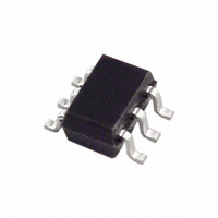
IC SWITCH SPDT SC70-6
Manufacturer
Analog Devices Inc
Type
Analog Switchr
Datasheet
1.ADG749BKSZ-REEL.pdf
(12 pages)
Specifications of ADG749BKSZ-REEL7
Function
Switch
Circuit
1 x SPDT
On-state Resistance
5 Ohm
Voltage Supply Source
Single Supply
Voltage - Supply, Single/dual (±)
1.8 V ~ 5.5 V
Current - Supply
0.001µA
Operating Temperature
-40°C ~ 85°C
Mounting Type
Surface Mount
Package / Case
6-TSSOP, SC-88, SOT-363
Analog Switch Type
SPDT
No. Of Channels
1
Bandwidth
200MHz
On State Resistance Max
2.5ohm
Turn Off Time
3ns
Turn On Time
7ns
Supply Voltage Range
1.8V To 5.5V
Multiplexer Configuration
Single SPDT
Number Of Inputs
1
Number Of Outputs
2
Number Of Channels
1
Analog Switch On Resistance
12@3VOhm
Analog Switch Turn On Time
10ns
Analog Switch Turn Off Time
4ns
Package Type
SC-70
Power Supply Requirement
Single
Single Supply Voltage (min)
1.8V
Single Supply Voltage (typ)
3/5V
Single Supply Voltage (max)
5.5V
Dual Supply Voltage (min)
Not RequiredV
Dual Supply Voltage (typ)
Not RequiredV
Dual Supply Voltage (max)
Not RequiredV
Power Dissipation
315mW
Supply Current
0.001mA
Mounting
Surface Mount
Pin Count
6
Operating Temp Range
-40C to 125C
Operating Temperature Classification
Automotive
Lead Free Status / RoHS Status
Lead free / RoHS Compliant
Lead Free Status / RoHS Status
Lead free / RoHS Compliant, Lead free / RoHS Compliant
Other names
ADG749BKSZ-REEL7TR
Available stocks
Company
Part Number
Manufacturer
Quantity
Price
Company:

Part Number:
ADG749BKSZ-REEL7
Manufacturer:
AD
Quantity:
500
Company:
Part Number:
ADG749BKSZ-REEL7
Manufacturer:
NSC
Quantity:
147
Part Number:
ADG749BKSZ-REEL7
Manufacturer:
ADI/亚德诺
Quantity:
20 000


ADG749
TABLE OF CONTENTS
Features .............................................................................................. 1
Applications ....................................................................................... 1
Functional Block Diagram .............................................................. 1
General Description ......................................................................... 1
Product Highlights ........................................................................... 1
Revision HistoryRevision History .................................................. 2
Specifications ..................................................................................... 3
Absolute Maximum Ratings ............................................................ 5
Pin Configuration and Function Descriptions ............................. 6
REVISION HISTORY
10/09—Rev. A to Rev. B
Updated Format .................................................................. Universal
Added Pb-Free Information to Table 3 .......................................... 5
Added Table 4 .................................................................................... 6
Updated Outline Dimensions ....................................................... 12
Changes to Ordering Guide .......................................................... 12
7/02—Rev. 0 to Rev. A.
Changes to Features .......................................................................... 1
Additions to Product Highlights .................................................... 1
Changes to Specifications ................................................................ 2
Edits to Absolute Maximum Ratings ............................................. 4
Changes to Terminology .................................................................. 4
Edits to Ordering Guide .................................................................. 4
Added new TPCs 4 and 5 ................................................................ 5
Added TPC 10 ................................................................................... 6
Test Circuits 6, 7, and 8 replaced .................................................... 7
Updated KS-6 Package Drawing ..................................................... 9
01/01—Revision 0: Initial Version
ESD Caution .................................................................................. 5
Rev. B | Page 2 of 12
Terminology .......................................................................................7
Typical Performance Characteristics ..............................................8
Test Circuits ..................................................................................... 10
Applications Information .............................................................. 11
Outline Dimensions ....................................................................... 12
ADG749 Supply Voltages .......................................................... 11
On Response vs. Frequency ...................................................... 11
Off Isolation ................................................................................ 11
Ordering Guide .......................................................................... 12
Related parts for ADG749BKSZ-REEL7
Image
Part Number
Description
Manufacturer
Datasheet
Request
R

Part Number:
Description:
Single SPDT
Manufacturer:
Analog Devices Inc
Datasheet:
Part Number:
Description:
IC SWITCH SPDT SC70-6
Manufacturer:
Analog Devices Inc
Datasheet:
Part Number:
Description:
IC SWITCH SPDT SC70-6
Manufacturer:
Analog Devices Inc
Datasheet:

Part Number:
Description:
±1.7g Dual-Axis IMEMS Accelerometer Evaluation Board
Manufacturer:
Analog Devices Inc
Datasheet:

Part Number:
Description:
Inertial Sensor Evaluation System
Manufacturer:
Analog Devices Inc
Datasheet:
Part Number:
Description:
Manufacturer:
Analog Devices Inc
Datasheet:
Part Number:
Description:
Manufacturer:
Analog Devices Inc
Datasheet:
Part Number:
Description:
Manufacturer:
Analog Devices Inc
Datasheet:
Part Number:
Description:
Manufacturer:
Analog Devices Inc
Datasheet:
Part Number:
Description:
Manufacturer:
Analog Devices Inc
Datasheet:
Part Number:
Description:
Manufacturer:
Analog Devices Inc
Datasheet:
Part Number:
Description:
Manufacturer:
Analog Devices Inc
Datasheet:
Part Number:
Description:
Manufacturer:
Analog Devices Inc
Datasheet: