BU4051BCF-E2 Rohm Semiconductor, BU4051BCF-E2 Datasheet - Page 15
BU4051BCF-E2
Manufacturer Part Number
BU4051BCF-E2
Description
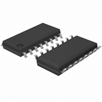
IC MUX/DEMUX 8X1 16SOP
Manufacturer
Rohm Semiconductor
Series
4000Br
Specifications of BU4051BCF-E2
Function
Multiplexer/Demultiplexer
Circuit
1 x 8:1
On-state Resistance
160 Ohm
Voltage Supply Source
Single Supply
Voltage - Supply, Single/dual (±)
3 V ~ 18 V
Current - Supply
15µA
Operating Temperature
-40°C ~ 85°C
Mounting Type
Surface Mount
Package / Case
16-SOIC (0.175", 4.4mm Width)
Lead Free Status / RoHS Status
Lead free / RoHS Compliant
Available stocks
Company
Part Number
Manufacturer
Quantity
Price
Company:

Part Number:
BU4051BCF-E2
Manufacturer:
ROHM
Quantity:
2 500
Company:
Part Number:
BU4051BCF-E2
Manufacturer:
ROHM
Quantity:
2 592
Part Number:
BU4051BCF-E2
Manufacturer:
ROHM/罗姆
Quantity:
20 000


5) BU4551B Series
●Notes for use
© 2009 ROHM Co., Ltd. All rights reserved.
BU4066BC,BU4066BCF,BU4066BCFV,BU4051BC,BU4051BCF,BU4051BCFV,BU4052BC,
BU4052BCF,BU4052BCFV,BU4053BC,BU4053BCF,BU4053BCFV,BU4551B,BU4551BF,BU4551BFV
www.rohm.com
CONT
1. Absolute maximum ratings
2. Connecting the power supply connector backward
3. Power Supply lines
4. GND voltage
5. Thermal design
6. Inter-pin shorts and mounting errors
7. Actions in strong electromagnetic field
8. Testing on application boards
9.Ground Wiring Pattern
VDD
VSS
VEE
W0
W1
X0
X1
Y0
Y1
Z0
Z1
An excess in the absolute maximum ratings, such as supply voltage, temperature range of operating conditions, etc., can
break down the devices, thus making impossible to identify breaking mode, such as short circuit or an open circuit. If any
over rated values will expect to exceed the absolute maximum ratings, consider adding circuit protection devices, such as
fuses.
Connecting of the power supply in reverse polarity can damage IC. Take precautions when connecting the power supply
lines. An external direction diode can be added.
Design PCB layout pattern to provide low impedance GND and supply lines. To obtain a low noise ground and supply line,
separate the ground section and supply lines of the digital and analog blocks. Furthermore, for all power terminals to ICs,
connect a capacitor between the power supply and the GND terminal. When applying electrolytic capacitors in the circuit,
not that capacitance characteristic values are reduced at low temperatures.
The potential of GND pin must be minimum potential in all operating conditions.
Use a thermal design that allows for a sufficient margin in light of the power dissipation (Pd) in actual operating conditions.
Use caution when positioning the IC for mounting on printed circuit boards. The IC may be damaged if there is any
connection error or if pins are shorted together.
Use caution when using the IC in the presence of a strong electromagnetic field as doing so may cause the IC to
malfunction.
When testing the IC on an application board, connecting a capacitor to a pin with low impedance subjects the IC to stress.
Always discharge capacitors after each process or step. Always turn the IC's power supply off before connecting it to or
remove it from a jig or fixture during the inspection process. Ground the IC during assembly steps as an antistatic measure.
Use similar precaution when transporting or storing the IC.
When using both small signal and large current GND patterns, it is recommended to isolate the two ground patterns,
placing a signal ground point at the ground potential of application so that the pattern wiring resistance and voltage
variations caused by large currents do not caused by large currents do not cause variations in the small signal ground
voltage. Be careful not to change the GND wiring pattern of any external components, either.
VEE
VSS
W1
X0
X1
Y0
X
Y
CONVERTER
1
2
3
4
5
6
7
8
LEVEL
X0
X1
X
Y
Y0
VEE
CONTROL
1Y
W0
Z1
Z0
Y1
CONTROL
W
Z
16
15
14
13
12
11
10
9
VDD
W0
W
Z
Z1
Z0
Y1
CONTROL
COMMON
COMMON
COMMON
COMMON
W
X
Y
Z
15/17
PIN FUNCTION
PIN No.
TRUTH TABLE
10
12
13
14
15
16
11
1
2
3
4
5
6
7
8
9
CONTROL
0
1
PIN NAME
CONTROL
VDD
VEE
VSS
W1
W0
X0
X1
Y0
Y1
Z0
Z1
W
X
Y
Z
I/O
I/O
I/O
I/O
I/O
I/O
I/O
I/O
I/O
I/O
I/O
I/O
I/O
-
-
I
-
Analog Switch Input / Output
Analog Switch Input / Output
Analog Switch Input / Output
Analog Switch Input / Output
Analog Switch Input / Output
Analog Switch Input / Output
Analog Switch Input / Output
Analog Switch Input / Output
Analog Switch Input / Output
Analog Switch Input / Output
ON SWITCH
W0,X0,Y0,Z0
W1,X1,Y1,Z1
Power Supply(+)
PIN FUNCTION
Power Supply(-)
Power Supply(-)
Control Input
Control Input
Control Input
Technical Note
2009.06 - Rev.A
Related parts for BU4051BCF-E2
Image
Part Number
Description
Manufacturer
Datasheet
Request
R

Part Number:
Description:
IC MUX/DEMUX 8X1 16DIP
Manufacturer:
Rohm Semiconductor
Datasheet:

Part Number:
Description:
Manufacturer:
Rohm Semiconductor
Datasheet:
Part Number:
Description:
Manufacturer:
Rohm Semiconductor
Datasheet:
Part Number:
Description:
Manufacturer:
Rohm Semiconductor
Datasheet:
Part Number:
Description:
Manufacturer:
Rohm Semiconductor
Datasheet:
Part Number:
Description:
Manufacturer:
Rohm Semiconductor
Datasheet:
Part Number:
Description:
Manufacturer:
Rohm Semiconductor
Datasheet:
Part Number:
Description:
Manufacturer:
Rohm Semiconductor
Datasheet:
Part Number:
Description:
Manufacturer:
Rohm Semiconductor
Datasheet:
Part Number:
Description:
Manufacturer:
Rohm Semiconductor
Datasheet:
Part Number:
Description:
Manufacturer:
Rohm Semiconductor
Datasheet:
Part Number:
Description:
Manufacturer:
Rohm Semiconductor
Datasheet:
Part Number:
Description:
Manufacturer:
Rohm Semiconductor
Datasheet: