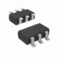
DG447DV-T1-E3 Vishay, DG447DV-T1-E3 Datasheet - Page 6

DG447DV-T1-E3
Manufacturer Part Number
DG447DV-T1-E3
Description
IC SWITCH DUAL SPST 6TSOP
Manufacturer
Vishay
Type
Analog Switchr
Datasheet
1.DG448DV-T1-E3.pdf
(8 pages)
Specifications of DG447DV-T1-E3
Function
Switch
Circuit
2 x SPST - NC
On-state Resistance
25 Ohm
Voltage Supply Source
Single, Dual Supply
Voltage - Supply, Single/dual (±)
7 V ~ 36 V, ± 4.5 V ~ 20 V
Current - Supply
16µA
Operating Temperature
-40°C ~ 85°C
Mounting Type
Surface Mount
Package / Case
6-TSOP (0.063", 1.60mm Width)
Number Of Switches
1
Switch Configuration
SPST
On Resistance (max)
45 Ohms
On Time (max)
175 ns
Off Time (max)
120 ns
Off Isolation (typ)
- 72 dB
Supply Voltage (max)
44 V
Supply Voltage (min)
7 V
Supply Current
0.016 mA
Maximum Power Dissipation
570 mW
Maximum Operating Temperature
+ 85 C
Mounting Style
SMD/SMT
Minimum Operating Temperature
- 40 C
Switch Current (typ)
30 mA
Analogue Switch Type
SPST
No. Of Channels
1
On State Resistance Max
25ohm
Turn Off Time
50ns
Turn On Time
100ns
Supply Voltage Range
± 4.5V To ± 20V
Operating Temperature Range
-40°C To
Package
6TSOP
Maximum On Resistance
45@12V Ohm
Maximum High Level Output Current
30 mA
Maximum Turn-off Time
120@12V ns
Maximum Turn-on Time
175@12V ns
Switch Architecture
SPST
Power Supply Type
Single|Dual
Lead Free Status / RoHS Status
Lead free / RoHS Compliant
Lead Free Status / RoHS Status
Lead free / RoHS Compliant, Lead free / RoHS Compliant
Other names
DG447DV-T1-E3TR
Available stocks
Company
Part Number
Manufacturer
Quantity
Price
Company:
Part Number:
DG447DV-T1-E3
Manufacturer:
Maxim
Quantity:
534
DG447, DG448
Vishay Siliconix
TYPICAL CHARACTERISTICS T
TEST CIRCUITS
V
www.vishay.com
6
O
is the steady state output with the switch on.
10 V
0.5
1.9
1.7
1.5
1.3
0.9
0.7
2.5
2.3
2.1
1.1
- 20
- 40
- 60
160
140
120
100
80
60
40
20
0
5
- 15
Input Switching Threshold vs. Supply Voltage
NO/NC
C
IN
C
GND
L
Charge Injection vs. Analog Voltage
L
(includes fixture and stray capacitance)
- 10
= 10 nF
10
V
O
= V
(Measured at COM pin)
S
- 5
Analog Voltage (V)
15
+ 15 V
- 15 V
V +
V -
COM
V+ (V)
R
0
L
R
+ r
20
V+ = + 15 V
V- = - 15 V
L
ON
R
300
L
5
A
Ω
= 25 °C, unless otherwise noted
V+ = + 12 V
V- = 0 V
25
V+ = + 12 V
V- = - 12 V
10
C
35 pF
Figure 1. Switching Time
L
30
V
O
15
Note:
Logic
Input
Switch
Input
Switch
Output
- 100
- 150
- 200
- 250
- 300
- 350
- 400
- 50
150
100
50
0
Logic input waveform is inverted for switches that have the
opposite logic sense.
- 15
V+ = + 15 V
V- = - 15 V
C
L
Charge Injection vs. Analog Voltage
3 V
0 V
0 V
V
- 10
= 10 nF
S
(Measured at NC or NO pin)
-5
V
t
Analog Voltage (V)
ON
O
50 %
90 %
0
S09-1260-Rev. C, 13-Jul-09
Document Number: 73854
5
V+ = + 12 V
V- = - 12 V
V+ = + 12 V
V- = 0 V
t
t
r
f
10
< 20 ns
< 20 ns
t
OFF
15


