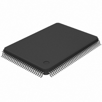
MAX4357ECD+D Maxim Integrated Products, MAX4357ECD+D Datasheet - Page 33

MAX4357ECD+D
Manufacturer Part Number
MAX4357ECD+D
Description
IC VIDEO CROSSPOINT SWIT 128TQFP
Manufacturer
Maxim Integrated Products
Datasheet
1.MAX4357ECDD.pdf
(42 pages)
Specifications of MAX4357ECD+D
Function
Video Crosspoint Switch
Circuit
1 x 32:16
Voltage Supply Source
Single, Dual Supply
Voltage - Supply, Single/dual (±)
5V, ± 3 V ~ 5 V
Operating Temperature
-40°C ~ 85°C
Mounting Type
Surface Mount
Package / Case
128-TQFP, 128-VQFP
Lead Free Status / RoHS Status
Lead free / RoHS Compliant
Other names
MAX4357ECD+
MAX4357ECD+
MAX4357ECD+
Figure 3. Mode 0, Individual Output Address Mode Timing and Programming Example
The wired-OR connection of the outputs shown in the
diagram is possible because the outputs of the IC
devices can be placed in a disabled, or high-imped-
ance-output state. This disable state of the output
buffers is designed for a maximum impedance vs. fre-
quency while maintaining a low-output capacitance.
These characteristics minimize the adverse loading
effects from the disabled outputs. Larger arrays are
constructed by extending this connection technique to
more devices.
Figure 6 shows an implementation requiring many out-
puts to be wired together. This creates a situation
where each output buffer sees not only the normal load
impedance, but also the disabled impedance of all the
other outputs. This impedance has a resistive and a
capacitive component. The resistive components
reduce the total effective load for the driving output.
Total capacitance is the sum of the capacitance of all
UPDATE
MODE
SCLK
DIN
32 x 16 Nonblocking Video Crosspoint Switch
t
SuMd
16-BIT INDIVIDUAL OUTPUT ADDRESS MODE:
FIRST BIT IS A DON'T CARE BIT, LAST 15 BITS CLOCKED INTO DIN WHEN MODE = 0, CREATES ADDRESS WORD; IC ADDRESS A3–A0 IS COMPARED TO DIN14–DIN11
WHEN UPDATE IS LOW; IF EQUAL, ADDRESSED OUTPUT IS UPDATED.
______________________________________________________________________________________
IC ADDRESS = 2
Driving a Capacitive Load
EXAMPLE OF 16-BIT SERIAL CONTROL WORD FOR OUTPUT CONTROL IN INDIVIDUAL OUTPUT ADDRESS MODE
OUTPUT ADDRESS = 9
the disabled outputs and is a function of the size of the
matrix. Also, as the size of the matrix increases, the
length of the PC board traces increases, adding more
capacitance. The output buffers have been designed to
drive more than 30pF of capacitance while still main-
taining a good AC response. Depending on the size of
the array, the capacitance seen by the output can
exceed this amount. There are several ways to improve
the situation. The first is to use more building-block
crosspoint devices to reduce the number of outputs
that need to be wired together (Figure 7).
In Figure 7, the additional devices are placed in a sec-
ond bank to multiplex the signals. This reduces the
number of wired-OR connections. Another solution is to
put a small resistor in series with the output before the
capacitive load to limit excessive ringing and oscilla-
tions. Figure 8 shows the Optimal Isolation Resistor vs.
Capacitive Load. A lowpass filter is created from the
series resistor and parasitic capacitance to ground.
OUTPUT (i) ENABLED, A
CONNECTED TO INPUT 16
with I/O Buffers
V
= +1V/V,
t
HdMd
33


