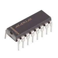
MAX305CPE+ Maxim Integrated Products, MAX305CPE+ Datasheet - Page 5

MAX305CPE+
Manufacturer Part Number
MAX305CPE+
Description
IC SWITCH DUAL DPST 16DIP
Manufacturer
Maxim Integrated Products
Datasheet
1.MAX303CPE.pdf
(8 pages)
Specifications of MAX305CPE+
Function
Switch
Circuit
2 x DPST - NO
On-state Resistance
35 Ohm
Voltage Supply Source
Single, Dual Supply
Voltage - Supply, Single/dual (±)
10 V ~ 30 V, ±4.5 V ~ 20 V
Operating Temperature
0°C ~ 70°C
Mounting Type
Through Hole
Package / Case
16-DIP (0.300", 7.62mm)
Number Of Switches
Dual
Switch Configuration
DPST
On Resistance (max)
35 Ohms
On Time (max)
150 ns
Off Time (max)
100 ns
Off Isolation (typ)
72 dB
Supply Voltage (max)
+/- 20 V
Supply Voltage (min)
+/- 4.5 V
Supply Current
0.01 uA
Maximum Power Dissipation
842 mW
Maximum Operating Temperature
+ 70 C
Mounting Style
Through Hole
Description/function
Analog Switch
Input Level
CMOS
Minimum Operating Temperature
0 C
Off State Leakage Current (max)
0.5 nA
Lead Free Status / RoHS Status
Lead free / RoHS Compliant
16, 9, 5, 4
16, 9, 5, 4
____________________Pin Descriptions
1, 8, 3, 6
1, 8, 3, 6
DIP/SO
DIP/SO
DIP/SO
10, 15
15, 10
15, 10
9, 16
1, 8
2-7
2-7
2-7
11
12
13
14
11
12
13
14
11
12
13
14
MAX301 PIN
MAX303 PIN
MAX305 PIN
Precision, Dual, High-Speed Analog Switches
1, 3-9, 11,
2, 4, 8, 10
2, 4, 8, 10
1, 3, 6, 9,
1, 3, 6, 9,
5, 7, 12,
5, 7, 12,
5, 7, 12,
13, 19
11, 16
19, 13
11, 16
19, 13
2, 10
LCC
LCC
LCC
16
20
14
15
17
18
14
15
17
18
20
14
15
17
18
20
________________________________________________________________________________________
IN2, IN1
IN1, IN2
IN1, IN2
COM1,
NAME
COM2
NAME
COM_
NAME
COM_
NC1,
GND
GND
NC_,
GND
N.C.
NC2
N.C.
NO_
N.C.
NO_
V+
V+
V+
V
V-
V
V-
V
V-
L
L
L
Drain (Analog Signal)
Not internally connected
Source (Analog Signal)
Digital Logic Inputs
Positive Supply-Voltage
Input—connected to
substrate
Logic Supply-Voltage Input
Ground
Negative Supply Voltage
Input
Drain (Analog Signal)
Not internally connected
Positive Supply-Voltage
Input—connected to
substrate
Logic Supply-Voltage Input
Ground
Negative Supply Voltage
Input
Digital Logic Inputs
Source (Analog Signal)
Drain (Analog Signal)
Not internally connected
Positive Supply-Voltage
Input—connected to
substrate
Logic Supply-Voltage Input
Ground
Negative Supply Voltage
Digital Logic Inputs
Source (Analog Signal)
FUNCTION
FUNCTION
FUNCTION
The MAX301/MAX303/MAX305 switches operate with
±4.5V to ±20V bipolar supplies and a +10V to +30V sin-
gle supply. In either case, analog signals ranging from V+
to V- can be switched. The Typical Operating
Characteristics graphs show the typical on-resistance
variation with analog signal and supply voltage. The usual
on-resistance temperature coefficent is 0.5%/°C (typ).
The MAX301/MAX303/MAX305 operate with a single pos-
itive supply or with bipolar supplies. The devices maintain
TTL compatibility with supplies anywhere in the ±4.5V to
±20V range as long as V
or another supply at voltages other than +5V, the devices
will operate at CMOS-logic level inputs.
Proper power-supply sequencing is recommended for all
CMOS devices. It is important not to exceed the absolute
maximum ratings because stresses beyond the listed rat-
ings may cause permanent damage to the devices.
Always sequence V+ on first, followed by VL, V-, and
logic inputs. If power-supply sequencing is not possible,
add two small signal diodes in series with the supply pins
for overvoltage protection (Figure 1). Adding diodes
reduces the analog signal range to 1V below V+ and 1V
below V-, but low switch resistance and low leakage char-
acteristics are unaffected. Device operation is
unchanged, and the difference between V+ to V- should
not exceed +44V.
Figure 1. Overvoltage Protection Using Blocking Diodes
__________Applications Information
V
g
Operation with Supply Voltages
NO_
L
= +5V. If V
Overvoltage Protection
V+
V-
Other than ±15V
L
is connected to V+
COM_
Logic Inputs
5


