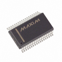
MAX4549EAX+ Maxim Integrated Products, MAX4549EAX+ Datasheet - Page 15

MAX4549EAX+
Manufacturer Part Number
MAX4549EAX+
Description
IC AUD/VIDCROSSPOINT SWIT 36SSOP
Manufacturer
Maxim Integrated Products
Datasheet
1.MAX4549EAX.pdf
(20 pages)
Specifications of MAX4549EAX+
Function
Audio/Video Crosspoint Switch
Circuit
3 x 3:2
On-state Resistance
35 Ohm
Voltage Supply Source
Single Supply
Voltage - Supply, Single/dual (±)
2.7 V ~ 5.5 V
Current - Supply
6µA
Operating Temperature
-40°C ~ 85°C
Mounting Type
Surface Mount
Package / Case
36-BSOP (0.300", 7.5mm Width)
Lead Free Status / RoHS Status
Lead free / RoHS Compliant
the same configuration. Any block that is not selected
in the command byte remains unchanged.
The MAX4548 uses a 2-wire I
face. The COM_ _ registers and the Clickless Mode
register use the “WriteByte” protocol, which consists of
an address byte, followed by a command byte, fol-
lowed by a data byte (Table 5). The Bias register uses
the “WriteWord” protocol, which consists of an address
byte, followed by a command byte, followed by a data
word (Table 6).
To address a given chip, the A0 and A1 bits in the
address byte must duplicate the values present at the
A0 and A1 pins of that chip. The rest of the address bits
must match those shown in Tables 5 and 6. The com-
mand and data-byte details are described in the
Command-Byte and Data-Byte Programming section.
The 2-wire serial interface requires only two I/O lines of
a standard microprocessor port. Figures 3, 4, and 5
detail the timing diagram for signals on the 2-wire bus,
Figure 6. 3-Wire Serial-Interface Communication
Figure 7. 3-Wire Serial-Interface Timing Details
DOUT
SCLK
DIN
CS
Serially Controlled, Triple 3x2 Audio/Video
SCLK
t
CSH
DIN
CS
______________________________________________________________________________________
t
DV
t
CSS
2-Wire Serial Interface
t
DS
2
C-compatible serial inter-
t
DH
C7
1
COMMAND BYTE
t
CL
t
CH
C0 D15
while Tables 5 and 6 detail the format of the signals.
The MAX4548 is a receive-only device and must be
controlled by the bus master device. A bus master
device communicates by transmitting the address byte
of the slave device over the bus and then transmitting
the desired information. Each transmission consists of
a start condition, a command byte, a data byte or word,
and finally a stop condition. The slave device acknowl-
edges the recognition of its address by pulling the SDA
line low for one clock period after the address byte is
transmitted. The slave device also issues a similar
acknowledgment after the command byte and again
after each data byte.
The bus master signals the beginning of a transmission
with a start condition by transitioning SDA from high to
low while SCL is high. When the master has finished
communicating with the slave, it issues a stop condition
by transitioning SDA from low to high while SCL is high.
The bus is then free for another transmission.
Crosspoint Switches
DATA BYTE
t
DO
D0
24
Start and Stop Conditions
t
CSH
t
TR
15


