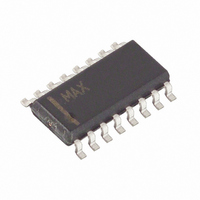
MAX312LCSE+ Maxim Integrated Products, MAX312LCSE+ Datasheet - Page 8

MAX312LCSE+
Manufacturer Part Number
MAX312LCSE+
Description
IC SWITCH QUAD SPST 16SOIC
Manufacturer
Maxim Integrated Products
Datasheet
1.MAX313LCSE.pdf
(14 pages)
Specifications of MAX312LCSE+
Function
Switch
Circuit
4 x SPST - NC
On-state Resistance
10 Ohm
Voltage Supply Source
Single, Dual Supply
Voltage - Supply, Single/dual (±)
4.5 V ~ 30 V, ±4.5 V ~ 20 V
Operating Temperature
0°C ~ 70°C
Mounting Type
Surface Mount
Package / Case
16-SOIC (0.154", 3.90mm Width)
Lead Free Status / RoHS Status
Lead free / RoHS Compliant
10 Ω Ω , Quad, SPST, +3V Logic-Compatible
Analog Switches
The MAX312L/MAX313L/MAX314L, having very low R
and very low R
well suited for low-distortion audio applications. The
Typical Operating Characteristics show Total Harmonic
Distortion (THD) vs. Frequency graphs for several signal
amplitudes and impedances. Higher source and load
impedances improve THD, but reduce off-isolation.
In 50Ω systems, the high-frequency on-response of
these parts extends from DC to above 100MHz with a
typical loss of -2dB. When the switch is turned off, how-
ever, it behaves like a capacitor, and off-isolation
decreases with increasing frequency. (Above 300MHz,
the switch actually passes more signal turned off than
turned on.) This effect is more pronounced with higher
source-and-load impedances.
Above 5MHz, circuit board layout becomes critical, and
it becomes difficult to characterize the response of the
switch independent of the circuit. The graphs shown in
the Typical Operating Characteristics were taken using a
50Ω source and load connected with BNC connectors.
8
6, 10, 16, 20
3, 8, 12, 13,
7, 9, 17, 19
1, 5, 11, 15
MAX312L
_______________________________________________________________________________________
—
—
—
18
14
—
2
4
Off-Isolation at High Frequencies
6, 10, 16, 20
PIN (TQFN)
3, 8, 12, 13,
7, 9, 17, 19
1, 5, 11, 15
MAX313L
ON
Applications Information
18
14
—
—
—
—
2
4
variation with signal amplitude, are
6, 10, 16, 20
3, 8, 12, 13,
7, 9, 17, 19
MAX314L
Low-Distortion Audio
11, 15
1, 5
18
14
—
—
—
2
4
COM4, COM3,
COM2, COM1
NC1, NC4,
NO1, NO4,
NC3, NC2
NO3, NO2
NO1, NO4
NC3, NC2
IN4, IN3,
IN2, IN1
NAME
GND
N.C.
V+
EP
V-
ON
Logic Inputs
Analog Signal Common Terminals
Analog Signal Normally Closed Terminals
Analog Signal Normally Open Terminals
Analog Signal Normally Open Terminals
Analog Signal Normally Closed Terminals
Negative Analog Supply Input (connect to GND for single-supply
operation)
Ground
No Connection. Not internally connected.
Positive Analog Supply Input
Exposed Pad. Connect EP to V+.
Most CMOS switches require specific power-supply
sequencing in order to prevent the devices from latching
up. The older MAX312/MAX313/MAX314 devices require
a proper power-supply sequence of V+, V
forth. Otherwise, it becomes necessary to add signal
diodes to the circuit in order to protect it from potential
latchups. The new MAX312L/MAX313L/MAX314L
devices eliminate the need for a V
user to utilize any power-up sequence that is required. It
is, however, important not to exceed the absolute maxi-
mum ratings because stresses beyond the listed ratings
may cause permanent damage to the devices.
TRANSISTOR COUNT: 92
PROCESS: CMOS
Pin Descriptions (continued)
Power-Supply Sequencing-Free
FUNCTION
Chip Information
L
pin and permit the
L
Operation
, V-, and so


