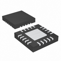
MAX4948ETG+ Maxim Integrated Products, MAX4948ETG+ Datasheet

MAX4948ETG+
Specifications of MAX4948ETG+
Related parts for MAX4948ETG+
MAX4948ETG+ Summary of contents
Page 1
... Small 25-Bump UCSP™ (2.5mm x 2.5mm) and 24-TQFN (4mm x 4mm) PART MAX4947EBA+* -40°C to +85°C Applications MAX4947ETG+ MAX4948EBA+* -40°C to +85°C MAX4948ETG+ * Future product—contact factory for availability. + Denotes lead-free package Exposed paddle. Typical Operating Circuit appears at end of data sheet. CB12 NO1 ...
Page 2
Hex SPDT Data Switch ABSOLUTE MAXIMUM RATINGS V to GND ...........................................................-0.3V to +6.0V CC All other pins to GND (Note 1) ......................-0. Continuous Current NO_, NC_, COM_ .......................................................±100mA Peak Current NO_, NC_, COM_ (pulsed at 1ms, 50% Duty ...
Page 3
ELECTRICAL CHARACTERISTICS (continued +2.7V to +5.5V -40°C to +85°C, unless otherwise noted. Typical values are PARAMETER SYMBOL COM_ Off-Leakage Current I COM DYNAMIC Turn-On Time Turn-Off Time Break-Before-Make HIGH-SPEED TIMING CHARACTERISTICS (rising ...
Page 4
Hex SPDT Data Switch ELECTRICAL CHARACTERISTICS (continued +2.7V to +5.5V -40°C to +85°C, unless otherwise noted. Typical values are Note 2: The algebraic convention is used. The most negative value is shown ...
Page 5
T = +25°C, unless otherwise noted CHARGE INJECTION vs. V COM 1nF (V) COM ...
Page 6
Hex SPDT Data Switch PIN MAX4947 MAX4948 TQFN UCSP TQFN — A1, C3 ...
Page 7
SIDE DOWN) MAX4947 COM3 GND NO4 NO3 CB34 A NC3 CB56 COM4 NC4 CB12 B NC2 COM5 NC5 GND COM2 C NC1 NO2 NO5 NC6 GND D COM1 NO1 NO6 COM6 V CC ...
Page 8
Hex SPDT Data Switch Detailed Description The MAX4947 triple DPDT and the MAX4948 hex SPDT analog switches operate from a single +1.8V to +5.5V supply. These devices are fully specified for +3V applications. The MAX4947/MAX4948 have a guaranteed 4Ω (typ) ...
Page 9
V MAX4947/ CC MAX4948 V CC NC_ V N_ COM_ NO_ CB_ LOGIC GND INPUT C INCLUDES FIXTURE AND STRAY CAPACITANCE. L Figure 2. Break-Before-Make-Interval TxD TxD 39Ω 50pF L |t ...
Page 10
Hex SPDT Data Switch MAX4947/ MAX4948 R GEN NC_ OR NO_ V GEN GND Figure 4. Charge Injection +5V 10nF CB_ COM1 MAX4947/ NC1 MAX4948 50Ω GND MEASUREMENTS ARE STANDARDIZED AGAINST SHORTS AT IC TERMINALS. ...
Page 11
CB CLK NO1 NC1 CMD NO2 NC2 DAT0 NO3 NC3 SD I/O 1 DAT1 NO4 NC4 DAT2 NO5 NC5 DAT3 NO6 NC6 CLK CMD DAT0 SD I/O 2 DAT1 DAT2 DAT3 ______________________________________________________________________________________ Hex SPDT Data Switch Typical Operating Circuit V ...
Page 12
Hex SPDT Data Switch (The package drawing(s) in this data sheet may not reflect the most current specifications. For the latest package outline information go to www.maxim-ic.com/packages.) 12 ______________________________________________________________________________________ Package Information PACKAGE OUTLINE, 5x5 UCSP 1 21-0096 H 1 ...
Page 13
... Maxim cannot assume responsibility for use of any circuitry other than circuitry entirely embodied in a Maxim product. No circuit patent licenses are implied. Maxim reserves the right to change the circuitry and specifications without notice at any time. Maxim Integrated Products, 120 San Gabriel Drive, Sunnyvale, CA 94086 408-737-7600 ____________________ 13 © 2007 Maxim Integrated Products ...


