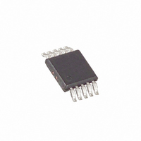
MAX4719EUB+ Maxim Integrated Products, MAX4719EUB+ Datasheet - Page 2

MAX4719EUB+
Manufacturer Part Number
MAX4719EUB+
Description
IC SWITCH DUAL SPDT 10UMAX
Manufacturer
Maxim Integrated Products
Datasheet
1.MAX4719EUB.pdf
(11 pages)
Specifications of MAX4719EUB+
Function
Switch
Circuit
2 x SPDT
On-state Resistance
20 Ohm
Voltage Supply Source
Single Supply
Voltage - Supply, Single/dual (±)
1.8 V ~ 5.5 V
Current - Supply
1µA
Operating Temperature
-40°C ~ 85°C
Mounting Type
Surface Mount
Package / Case
10-MSOP, Micro10™, 10-uMAX, 10-uSOP
Number Of Switches
Dual
Switch Configuration
SPDT
On Resistance (max)
25 Ohms
On Time (max)
100 ns
Off Time (max)
50 ns
Off Isolation (typ)
- 80 dB
Bandwidth
300 MHz
Supply Voltage (max)
5.5 V
Supply Voltage (min)
1.8 V
Supply Current
1 uA
Maximum Power Dissipation
444 mW
Maximum Operating Temperature
+ 85 C
Mounting Style
SMD/SMT
Minimum Operating Temperature
- 40 C
Off State Leakage Current (max)
2 nA
Lead Free Status / RoHS Status
Lead free / RoHS Compliant
(All Voltages Referenced to GND)
V+, IN_...................................................................-0.3V to +6.0V
COM_, NO_, NC_ (Note 1) ...........................-0.3V to (V+ + 0.3V)
Continuous Current COM_, NO_, NC_ ...........................±100mA
Peak Current COM_, NO_, NC_
Continuous Power Dissipation (T
20 , 300MHz Bandwidth, Dual SPDT Analog
Switch in UCSP
ABSOLUTE MAXIMUM RATINGS
Note 1: Signals on COM_, NO_, or NC_ exceeding V+ or GND are clamped by internal diodes. Limit forward-diode current to maxi-
Note 2: This device is constructed using a unique set of packaging techniques that impose a limit on the thermal profile the device
Stresses beyond those listed under “Absolute Maximum Ratings” may cause permanent damage to the device. These are stress ratings only, and functional
operation of the device at these or any other conditions beyond those indicated in the operational sections of the specifications is not implied. Exposure to
absolute maximum rating conditions for extended periods may affect device reliability.
ELECTRICAL CHARACTERISTICS—Single +3V Supply
(V+ = +2.7V to +3.6V, V
T
2
Analog Signal Range
ANALOG SWITCH
On-Resistance (Note 5)
On-Resistance Match Between
Channels (Notes 5, 6)
On-Resistance Flatness
(Note 7)
NO_, NC_ Off-Leakage Current
(Note 8)
COM_ On-Leakage Current
(Note 8)
DYNAMIC CHARACTERISTICS
Turn-On Time
A
(pulsed at 1ms, 10% duty cycle)................................±200mA
10-Pin µMAX (derate 5.6mW/°C above +70°C) ...........444mW
12-Bump UCSP (derate 11.4mW/°C above +70°C) ....909mW
= +25°C, unless otherwise noted.) (Notes 3, 4)
_______________________________________________________________________________________
mum current rating.
can be exposed to during board level solder attach and rework. This limit permits only the use of the solder profiles recom-
mended in the industry standard specification, JEDEC 020A, paragraph 7.6, table 3 for IR/VPR and convection reflow.
Preheating is required. Hand or wave soldering is not allowed.
PARAMETER
IH
= +1.4V, V
A
= +70°C)
V
R
I
I
SYMBOL
I
COM_(ON)
NO_
NO_(OFF),
NC_(OFF)
V
FLAT(ON)
IL
COM_
R
t
R
ON
, V
ON
= +0.5V, T
ON
NC_
,
V+ = 2.7V, I
V
V+ = 2.7V, I
V
V+ = 2.7V, I
V
V+ = 3.6V, V
V
V+ = 3.6V, V
V
floating
V
R
NO_
NO_
NO_
NO_
NO_
NO_
L
= 300 , C
A
, V
= T
or V
or V
or V
or V
or V
NC_
CONDITIONS
MIN
NC_
NC_
NC_
NC_
NC_
COM_
COM_
COM_
= 1.5V;
COM_
COM_
L
to T
= 1.5V
= 1.5V
= 1.0V, 1.5V, 2.0V
= 3.3V, 0.3V
= 0.3V, 3.3V, or
= 35pF, Figure 1
MAX
= 10mA;
= 10mA;
= 10mA;
= 0.3V, 3.3V;
= 0.3V, 3.3V;
ESD Method 3015.7 ...............................................................2kV
Operating Temperature Range ...........................-40°C to +85°C
Junction Temperature ......................................................+150°C
Storage Temperature Range .............................-65°C to +150°C
Lead Temperature (soldering, 10s) .................................+300°C
Bump Temperature (soldering) (Note 2)
, unless otherwise noted. Typical values are at V+ = +3.0V,
Infrared (15s) ...............................................................+220°C
Vapor Phase (60s) .......................................................+215°C
T
T
T
T
T
T
T
+25°C
+25°C
+25°C
+25°C
+25°C
+25°C
T
T
T
T
T
T
T
MIN
MIN
MIN
MIN
MIN
MIN
MIN
T
MAX
MAX
MAX
MAX
MAX
MAX
MAX
A
to
to
to
to
to
to
to
MIN
-0.5
-1
-1
-2
0
TYP
0.15
0.01
0.01
0.6
14
40
MAX
+0.5
100
V+
0.4
0.5
1.2
1.5
20
25
+1
+1
+2
80
UNITS
nA
nA
ns
V


