ISL54211IRTZ Intersil, ISL54211IRTZ Datasheet - Page 19
ISL54211IRTZ
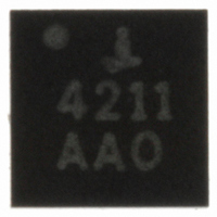
Manufacturer Part Number
ISL54211IRTZ
Description
IC SWITCH DUAL SPDT HS 10-TDFN
Manufacturer
Intersil
Datasheet
1.ISL54211IRUZ-T.pdf
(19 pages)
Specifications of ISL54211IRTZ
Function
Switch
Circuit
2 x SPDT
Voltage Supply Source
Single Supply
Voltage - Supply, Single/dual (±)
2.7 V ~ 5 V
Operating Temperature
-40°C ~ 85°C
Mounting Type
Surface Mount
Package / Case
10-TDFN Exposed Pad
Rohs Compliant
Yes
Lead Free Status / RoHS Status
Lead free / RoHS Compliant


Ultra Thin Quad Flat No-Lead Plastic Package (UTQFN)
Intersil products are sold by description only. Intersil Corporation reserves the right to make changes in circuit design, software and/or specifications at any time without
notice. Accordingly, the reader is cautioned to verify that data sheets are current before placing orders. Information furnished by Intersil is believed to be accurate and
reliable. However, no responsibility is assumed by Intersil or its subsidiaries for its use; nor for any infringements of patents or other rights of third parties which may result
from its use. No license is granted by implication or otherwise under any patent or patent rights of Intersil or its subsidiaries.
NX (b)
5
SECTION "C-C"
SEATING PLANE
INDEX AREA
0.05 C
0.10 C
2X
1.80
2X
All Intersil U.S. products are manufactured, assembled and tested utilizing ISO9000 quality systems.
6
1.00
0.10 C
PIN #1 ID
0.50
(A1)
(DATUM A)
Intersil Corporation’s quality certifications can be viewed at www.intersil.com/design/quality
A
0.20
0.10 C
L1
10
A1
For information regarding Intersil Corporation and its products, see www.intersil.com
N
LAND PATTERN
BOTTOM VIEW
SIDE VIEW
C C
2.20
1.00
0.60
TOP VIEW
0.40
19
1
1
7
D
e
e
2
2
C L
NX L
0.20
5
0.40
NX b
10X
A
(DATUM B)
C
TERMINAL TIP
0.10 M C A B
0.05 M C
B
E
5
L
ISL54211
L10.1.8x1.4A
10 LEAD ULTRA THIN QUAD FLAT NO-LEAD PLASTIC
PACKAGE
NOTES:
10. For additional information, to assist with the PCB Land Pattern
1. Dimensioning and tolerancing conform to ASME Y14.5-1994.
2. N is the number of terminals.
3. Nd and Ne refer to the number of terminals on D and E side,
4. All dimensions are in millimeters. Angles are in degrees.
5. Dimension b applies to the metallized terminal and is measured
6. The configuration of the pin #1 identifier is optional, but must be
7. Maximum package warpage is 0.05mm.
8. Maximum allowable burrs is 0.076mm in all directions.
9. JEDEC Reference MO-255.
SYMBOL
respectively.
between 0.15mm and 0.30mm from the terminal tip.
located within the zone indicated. The pin #1 identifier may be
either a mold or mark feature.
Design effort, see Intersil Technical Brief TB389.
A1
A3
Nd
Ne
L1
A
D
E
N
b
e
L
θ
0.45
0.15
1.75
1.35
0.35
0.45
MIN
0
-
MILLIMETERS
0.127 REF
NOMINAL
0.40 BSC
0.50
0.20
1.80
1.40
0.40
0.50
10
2
3
-
-
0.55
0.05
0.25
1.85
1.45
0.45
0.55
MAX
12
August 25, 2008
Rev. 3 6/06
NOTES
FN6662.1
5
2
3
3
4
-
-
-
-
-
-
-
-
Related parts for ISL54211IRTZ
Image
Part Number
Description
Manufacturer
Datasheet
Request
R

Part Number:
Description:
Mp3/usb 2.0 High Speed Switch With Negative Signal Handling/click And Pop Suppression
Manufacturer:
Intersil Corporation
Datasheet:
Part Number:
Description:
Intersil Corporation [CMOS Serial Controller Interface]
Manufacturer:
Intersil Corporation
Datasheet:
Part Number:
Description:
Manufacturer:
Intersil Corporation
Datasheet:
Part Number:
Description:
357-036-542-201 CARDEDGE 36POS DL .156 BLK LOPRO
Manufacturer:
Intersil Corporation
Datasheet:
Part Number:
Description:
1024-Word x 4-Bit LSI Static RAM
Manufacturer:
Intersil Corporation
Datasheet:
Part Number:
Description:
General Purpose NPN Transistor Arrays FN341.4
Manufacturer:
Intersil Corporation
Datasheet:
Part Number:
Description:
CMOS 16-Bit Microprocessor
Manufacturer:
Intersil Corporation
Datasheet:
Part Number:
Description:
Manufacturer:
Intersil Corporation
Datasheet:
Part Number:
Description:
Manufacturer:
Intersil Corporation
Datasheet:
Part Number:
Description:
Manufacturer:
Intersil Corporation
Datasheet:
Part Number:
Description:
Manufacturer:
Intersil Corporation
Datasheet:
Part Number:
Description:
CMOS 6-Bit Latch and Decoder Memory Interfaces
Manufacturer:
Intersil Corporation
Datasheet:
Part Number:
Description:
CA3046General Purpose NPN Transistor Arrays
Manufacturer:
Intersil Corporation
Datasheet:
Part Number:
Description:
Manufacturer:
Intersil Corporation
Datasheet:
Part Number:
Description:
TR909 DLC/FLC SLIC with Low Power Standby
Manufacturer:
Intersil Corporation
Datasheet: