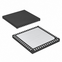
PI3L500ZFE Pericom Semiconductor, PI3L500ZFE Datasheet - Page 3

PI3L500ZFE
Manufacturer Part Number
PI3L500ZFE
Description
IC ETHERNET SWITCH OCTAL 56TQFN
Manufacturer
Pericom Semiconductor
Datasheet
1.PI3L500ZFE.pdf
(7 pages)
Specifications of PI3L500ZFE
Function
Ethernet Switch
Circuit
8 x 2:1
On-state Resistance
6.5 Ohm
Voltage Supply Source
Single Supply
Voltage - Supply, Single/dual (±)
3 V ~ 3.6 V
Current - Supply
0.5µA
Operating Temperature
-40°C ~ 85°C
Mounting Type
Surface Mount
Package / Case
56-TQFN
Number Of Channels
8 Channel
On Resistance (max)
4 Ohms (Typ) @ 3.3 V
Propagation Delay Time
0.25 ns (Typ)@3.3V@- 40C to 85C
On Time (max)
15 ns @ 3.3 V @ - 40 C to 85 C
Off Time (max)
9 ns @ 3.3 V @ - 40 C to 85 C
Supply Voltage (max)
3.6 V
Supply Voltage (min)
3 V
Maximum Power Dissipation
500 mW
Maximum Operating Temperature
+ 85 C
Minimum Operating Temperature
- 40 C
Mounting Style
SMD/SMT
Lead Free Status / RoHS Status
Lead free / RoHS Compliant
Available stocks
Company
Part Number
Manufacturer
Quantity
Price
Part Number:
PI3L500ZFE
Manufacturer:
PI
Quantity:
20 000
Part Number:
PI3L500ZFEX
Manufacturer:
PERICOM
Quantity:
20 000
DC Electrical Characteristics for 1000 Base-T Ethernet Switching over Operating Range
(T
Notes:
1.
2.
3.
DC Electrical Characteristics for 10/100 Base-T Ethernet Switching over Operating Range
(T
Notes:
1.
2.
3.
Paramenter
A
A
Paramenter
R
R
= –40°C to +85°C, V
= –40°C to +85°C, V
FLAT(ON)
For max. or min. conditions, use appropriate value specifi ed under Electrical Characteristics for the applicable device type.
Typical values are at V
Measured by the voltage drop between A and B pins at indicated current through the switch. ON resistance is determined by the lower of the
voltages on the two (A & B) pins.
ΔR
FLAT(ON)
R
∆R
V
V
V
R
I
I
V
V
V
IH
ON
I
IL
I
IH
IL
IK
IH
ON
ON
IL
07-0075
IH
IK
IL
ON
Input HIGH Voltage
Input LOW Voltage
Clamp Diode Voltage
Input HIGH Current
Input LOW Current
Switch On-Resistance
On-Resistance Flatness
On-Resistance match from center
ports to any other port
Input HIGH Voltage
Input LOW Voltage
Clamp Diode Voltage
Input HIGH Current
Input LOW Current
Switch On-Resistance
On-Resistance Flatness
On-Resistance match from cen-
ter ports to any other port
CC
CC
CC
CC
Description
Description
= 3.3V, T
= 3.3V, T
= 3.3V ±10%)
= 3.3V ±10%)
A
A
= 25°C ambient and maximum loading.
= 25°C ambient and maximum loading.
(3)
(3)
(3)
(3)
(3)
(3)
Guaranteed HIGH level (Control Pins)
Guaranteed LOW level (Control Pins)
V
V
V
V
I
V
I
V
I
Guaranteed HIGH level (Control Pins)
Guaranteed LOW level (Control Pins)
V
V
V
V
I
V
I
V
I
IN
IN
IN
IN
IN
IN
CC
CC
CC
CC
CC
CC
CC
CC
CC
CC
CC
CC
= –10mA to –30mA
= –10mA to –30mA
= –10mA to –30mA
= –40mA
= –40mA
= –40mA
= Max., V
= Max., I
= Max., V
= Min., 1.25V ≤ V
= Min., V
= Min., 1.25V ≤ V
= Max., I
= Max., V
= Max., V
= Min., 1.5V ≤ V
= Min., V
= Min., 1.5V ≤ V
Test Conditions
Test Conditions
3
IN
IN
IN
IN
IN
IN
IN
IN
= –18mA
@ 1.25V and V
= –18mA
= V
= GND
@ 1.5V and V
= V
= GND
Gigabit Ethernet LAN Switch w/Single Enable
CC
CC
IN
IN
IN
IN
≤ V
≤ V
≤ V
≤ V
(1)
(1)
CC
CC
CC
CC
CC
CC
3.3V, 8-Channel, 2:1 Mux/DeMux
Min.
Min.
–0.5
–0.5
2.0
2.0
Typ.
Typ.
–0.7
–0.7
4.0
0.5
0.4
4.0
0.5
0.4
(2)
(2)
PS8719D
Max.
Max.
–1.2
–1.2
0.8
6.5
1.0
±5
±5
0.8
6.5
1.0
±5
±5
–
PI3L500
Units
Units
μA
μA
Ω
Ω
V
V
03/23/07


