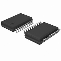
PI2DBS212QE Pericom Semiconductor, PI2DBS212QE Datasheet - Page 2

PI2DBS212QE
Manufacturer Part Number
PI2DBS212QE
Description
IC MUX/DEMUX 2X2 20QSOP
Manufacturer
Pericom Semiconductor
Datasheet
1.PI2DBS212ZHE.pdf
(11 pages)
Specifications of PI2DBS212QE
Function
Multiplexer/Demultiplexer
Circuit
1 x 2:2
On-state Resistance
10 Ohm
Current - Supply
300µA
Operating Temperature
-40°C ~ 85°C
Mounting Type
Surface Mount
Package / Case
20-QSOP
Lead Free Status / RoHS Status
Lead free / RoHS Compliant
Available stocks
Company
Part Number
Manufacturer
Quantity
Price
Company:
Part Number:
PI2DBS212QE
Manufacturer:
PYRAMISCORP
Quantity:
2 500
Maximum Ratings
(Above which useful life may be impaired. For user guide lines, not tested.)
DC Electrical Characteristics over 1.8V Operating Range
Notes:
1.
2.
Power Supply Characteristics over 1.8V Operating Range
Notes:
1.
2.
Switching Characteristics over 1.8V Operating Range
Notes:
1.
t
t
t
t
t
Parameters
PZH
PHZ
b-b
ch-ch
PD
Storage Temperature....................................–65°C to +150°C
Supply Voltage to Ground Potential...............–0.5V to +2.5V
DC Input Voltage ............................................–0.5V to V
DC Output Current......................................................120mA
Power Dissipation...........................................................0.5W
Parameter
Parameter
For max. or min. conditions, use appropriate value specifi ed under Electrical Characteristics for the applicable device type.
For Max. or Min. conditions, use appropriate value specifi ed under Electrical Characteristics for the applicable device type.
Typical values are at V
For Max. or Min. conditions, use appropriate value specifi ed under Electrical Characteristics for the applicable device type.
Typical values are at V
, t
, t
I
R
C
DD
V
V
V
I
I
PZL
PLZ
IH
ON
ON
09-0008
IL
IH
IK
IL
Quiescent Power Supply Current
Line Enable Time - SEL to A
Line Disable Time - SEL to A
Bit-to-bit skew, within same differential pair
Channel-to-channel timing skew
Propagation Delay, A to B or C / B or C to A
Input HIGH Voltage
Input LOW Voltage
Clamp Diode Voltage
Input HIGH Current
Input LOW Current
ON Resistance
Capacitance ON (A/B)
DD
DD
Description
= 1.8V, T
= 1.8V, T
Description
A
A
= 25°C ambient and maximum loading.
= 25°C ambient and maximum loading.
Description
N
N
, B
, B
N
N
V
V
Guaranteed HIGH level
Guaranteed LOW level
V
V
V
V
40mA
V
DD
DD
DD
DD
DD
DD
IN
= 0, V
= 2.0, V
(1)
= Max., I
= Max., V
= Max., V
= Min., V
DD
Test Conditions
DD
2
IN
Test Conditions
= 1.8V
IN
Note:
Stresses greater than those listed under MAX I MUM RAT INGS may cause
permanent damage to the de vice. This is a stress rating only and func-
tion al op er a tion of the device at these or any other conditions above those
indicated in the operational sections of this spec i fi ca tion is not implied.
Exposure to absolute max i mum rating con di tions for extended periods
may affect re li abil i ty.
IN
and V
IN
IN
(T A = -40°C to +85°C, V DD = 1.8V ±10%)
= –18mA
= 1.3V, I
= V
= GND
2-Differential Channel, 2:1 Mux/DeMux Switch
2.0GHz, Differential Broadband Signal Switch,
(T A = -40°C to +85°C, V DD = 1.8V ±10%)
(T A = -40°C to +85°C, V DD = 1.8V ±10%)
SEL
DD
(1)
= GND or
IN
=
(1)
0.65 x V
Min.
–0.5
Min.
0.5
0.5
50
Min.
DD
Typ.
–0.7
3.5
Typ.
Typ.
300
(2)
(2)
0.35 x V
PS8921B
Max.
Max.
150
–1.2
8.0
4.0
Max.
12
±5
±5
10
5
400
PI2DBS212
DD
Units
Units
Units
ns
ps
Ohm
08/20/09
μA
μA
pF
V


