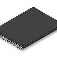
S29GL128S10TFI010 Spansion Inc., S29GL128S10TFI010 Datasheet - Page 69

S29GL128S10TFI010
Manufacturer Part Number
S29GL128S10TFI010
Description
Flash 128 MBIT 3V 100NS PAGE MODE FLASH
Manufacturer
Spansion Inc.
Datasheet
1.S29GL128S10TFI010.pdf
(97 pages)
Specifications of S29GL128S10TFI010
Data Bus Width
16 bit
Memory Type
Flash
Memory Size
128 Mbit
Architecture
Uniform
Timing Type
Asynchronous
Interface Type
CFI
Access Time
100 ns
Supply Voltage (max)
3.6 V
Supply Voltage (min)
2.7 V
Maximum Operating Current
100 mA
Operating Temperature
- 40 C to + 85 C
Mounting Style
SMD/SMT
Package / Case
TSOP-56
Lead Free Status / Rohs Status
Compliant
Available stocks
Company
Part Number
Manufacturer
Quantity
Price
Part Number:
S29GL128S10TFI010
Manufacturer:
SPANSIO
Quantity:
20 000
8.5
February 11, 2011 S29GL_128S_01GS_00_01
8.4.3
8.5.1
8.5.2
8.5.3
Write
Page Read
Asynchronous Write
Write Pulse “Glitch” Protection
Logical Inhibit
to the Write state. If CE# returns High, the interface goes to the Standby state. Back to Back accesses, in
which CE# remains Low between accesses, requires an address change to initiate the second access.
See
After a Random Read access is completed, if CE# remains Low, OE# remains Low, the
signals remain stable, and any of the A3 to A0 address signals change, a new access within the same Page
begins. The Page Read completes much faster (t
When WE# goes Low after CE is Low, there is a transition from one of the read states to the Write state. If
WE# is Low before CE# goes Low, there is a transition from the Standby state directly to the Write state
without beginning a read access.
When CE# is Low, OE# is High, and WE# goes Low, a write data transfer begins. Note, OE# and WE# should
never be Low at the same time to ensure no data bus contention between the host system and memory.
When the asynchronous write cycle timing requirements are met the WE# can go High to capture the address
and data values in to EAC command memory.
Address is captured by the falling edge of WE# or CE#, whichever occurs later. Data is captured by the rising
edge of WE# or CE#, whichever occurs earlier.
When CE# is Low before WE# goes Low and stays Low after WE# goes High, the access is called a WE#
controlled Write. When WE# is High and CE# goes High, there is a transition to the Standby state. If CE#
remains Low and WE# goes High, there is a transition to the Read with Output Disable state.
When WE# is Low before CE# goes Low and remains Low after CE# goes High, the access is called a CE#
controlled Write. A CE# controlled Write transitions to the Standby state.
If WE# is Low before CE# goes Low, the write transfer is started by CE# going Low. If WE# is Low after CE#
goes High, the address and data are captured by the rising edge of CE#. These cases are referred to as CE#
controlled write state transitions.
Write followed by Read accesses, in which CE# remains Low between accesses, requires an address
change to initiate the following read access.
Back to Back accesses, in which CE# remains Low between accesses, requires an address change to initiate
the second access.
The EAC command memory array is not readable by the host system and has no ASO. The EAC examines
the address and data in each write transfer to determine if the write is part of a legal command sequence.
When a legal command sequence is complete the EAC will initiate the appropriate EA.
Noise pulses of less than 5 ns (typical) on WE# will not initiate a write cycle.
Write cycles are inhibited by holding OE# at V
and WE# must be Low (V
D a t a
Asynchronous Read Operations on page
S h e e t
IL
( A d v a n c e
) while OE# is High (V
GL-S MirrorBit
I n f o r m a t i o n )
IL
78.
, or CE# at V
®
PACC
IH
Family
).
) than a Random Read access.
IH
, or WE# at V
IH
. To initiate a write cycle, CE#
A
MAX
to A4 address
69


