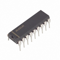
MAX350CPN+ Maxim Integrated Products, MAX350CPN+ Datasheet - Page 17

MAX350CPN+
Manufacturer Part Number
MAX350CPN+
Description
IC MULTIPLEXER DUAL 4X1 18DIP
Manufacturer
Maxim Integrated Products
Datasheet
1.MAX350CPN.pdf
(20 pages)
Specifications of MAX350CPN+
Function
Multiplexer
Circuit
2 x 4:1
On-state Resistance
100 Ohm
Voltage Supply Source
Single, Dual Supply
Voltage - Supply, Single/dual (±)
2.7 V ~ 16 V, ±2.7 V ~ 8 V
Current - Supply
1µA
Operating Temperature
0°C ~ 70°C
Mounting Type
Through Hole
Package / Case
18-DIP (0.300", 7.62mm)
Lead Free Status / RoHS Status
Lead free / RoHS Compliant
The MAX349/MAX350 construction is typical of most
CMOS analog switches. It has three supply pins: V+, V-
and GND. V+ and V- are used to drive the internal
CMOS switches, and they set the limits of the analog
voltage on any switch. Reverse ESD-protection diodes
are internally connected between each analog signal
pin and both V+ and V-. If any analog signal exceeds
V+ or V-, one of these diodes will conduct. During normal
operation, these (and other) reverse-biased ESD diodes
leak, forming the only current drawn from V+ or V-.
Figure 6. Addressable Serial Interface
Figure 7. Differential Multiplexer Input Control
SCLK
DIN
SCLK
CS1
CS2
CS3
DIN
Power-Supply Considerations
______________________________________________________________________________________
SW4
8-Channel/Dual 4-Channel Multiplexers
D4
CS
SCLK
DIN
MAX349
MAX350
FOUR CLOCK
PULSES
Serially Controlled, Low-Voltage,
SW0
Overview
D0
CS
SCLK
DIN
MAX349
MAX350
Virtually all the analog leakage current is through the
ESD diodes. Although the ESD diodes on a given sig-
nal pin are identical, and therefore fairly well balanced,
they are reverse biased differently. Each is biased by
either V+ or V- and the analog signal. This means their
leakages vary as the signal varies. The difference in the
two diode leakages to the V+ and V- pins constitutes
the analog signal-path leakage current. All analog leak-
age current flows to the supply terminals, not to the
other switch terminal. This is why both sides of a given
switch can show leakage currents of either the same or
opposite polarity.
There is no connection between the analog signal
paths and GND.
V+ and GND power the internal logic and logic-level
translators, and set both the input and output logic lim-
its. The logic-level translators convert the logic levels to
switched V+ and V- signals to drive the analog signal
gates. This drive signal is the only connection between
the logic supplies (and signals) and the analog sup-
plies. V+ and V- have ESD-protection diodes to GND.
The logic-level inputs and output have ESD protection
to V+ and to GND.
The logic-level thresholds are CMOS and TTL compati-
ble when V+ is +5V. As V+ rises, the threshold increases
slightly. Therefore, when V+ reaches +12V, the threshold
is about 3.1V; above the TTL-guaranteed high-level mini-
mum of 2.8V, but still compatible with CMOS outputs.
CS
SCLK
DIN
MAX349
MAX350
TO OTHER
SERIAL
DEVICES
17


