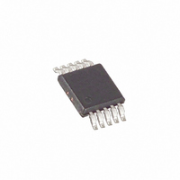
MAX4685EUB+ Maxim Integrated Products, MAX4685EUB+ Datasheet - Page 7

MAX4685EUB+
Manufacturer Part Number
MAX4685EUB+
Description
IC SWITCH DUAL SPDT 10UMAX
Manufacturer
Maxim Integrated Products
Datasheet
1.MAX4684EBCT.pdf
(10 pages)
Specifications of MAX4685EUB+
Function
Switch
Circuit
2 x SPDT
On-state Resistance
800 mOhm
Voltage Supply Source
Single Supply
Voltage - Supply, Single/dual (±)
1.8 V ~ 5.5 V
Operating Temperature
-40°C ~ 85°C
Mounting Type
Surface Mount
Package / Case
10-MSOP, Micro10™, 10-uMAX, 10-uSOP
Number Of Switches
Dual
Switch Configuration
SPDT
On Resistance (max)
0.8 Ohms
On Time (max)
60 ns
Off Time (max)
40 ns
Off Isolation (typ)
- 64 dB
Supply Voltage (max)
5.5 V
Supply Voltage (min)
1.8 V
Maximum Power Dissipation
444 mW
Maximum Operating Temperature
+ 85 C
Mounting Style
SMD/SMT
Description/function
Analog Switch
Minimum Operating Temperature
- 40 C
Off State Leakage Current (max)
10 nA
Lead Free Status / RoHS Status
Lead free / RoHS Compliant
For general UCSP package information and PC layout
considerations, please refer to the Maxim Application
Note (Wafer-Level Ultra-Chip-Board-Scale Package).
The chip-scale package (UCSP) represents a unique
packaging form factor that may not perform equally to a
packaged product through traditional mechanical relia-
bility tests. UCSP reliability is integrally linked to the
user’s assembly methods, circuit board material, and
usage environment. The user should closely review
these areas when considering use of a UCSP package.
Performance through Operating Life Test and Moisture
Resistance remains uncompromised as it is primarily
determined by the wafer-fabrication process.
Figure 2. Switching Time
Figure 3. Break-Before-Make Interval
MAX4684
MAX4685
LOGIC
INPUT
MAX4684
MAX4685
LOGIC
INPUT
V
V
N_
IN_
UCSP Package Consideration
_______________________________________________________________________________________
C
V
OUT
L
INCLUDES FIXTURE AND STRAY CAPACITANCE.
NO_
OR NC
IN_
= V
C
GND
L
NC_
NO_
IN_
INCLUDES FIXTURE AND STRAY CAPACITANCE.
N_
(
R
L
R
+ R
L
UCSP Reliability
GND
ON
)
0.5 Ω Ω /0.8 Ω Ω Low-Voltage, Dual SPDT
V+
V+
V+
COM_
V+
COM_
R
50Ω
L
R
50Ω
L
V
OUT
C
35pF
L
C
35pF
V
Analog Switches in UCSP
L
OUT
Mechanical stress performance is a greater considera-
tion for a UCSP package. UCSPs are attached through
direct solder contact to the user’s PC board, foregoing
the inherent stress relief of a packaged product lead
frame. Solder joint contact integrity must be consid-
ered. Information on Maxim’s qualification plan, test
data, and recommendations are detailed in the UCSP
application note, which can be found on Maxim’s web-
site at www.maxim-ic.com.
PROCESS: BiCMOS
SWITCH
OUTPUT
LOGIC
INPUT
Test Circuits/Timing Diagrams
LOGIC
INPUT
V
OUT
V
V
IH
IL
0
V
V
IH
IL
LOGIC INPUT WAVEFORMS INVERTED FOR SWITCHES
THAT HAVE THE OPPOSITE LOGIC SENSE.
V
t
50%
50%
ON
OUT
0.9 x V
t
Chip Information
D
0UT
t
OFF
0.9 x V
t r < 5ns
t f < 5ns
0.9 x V
OUT
OUT
7


