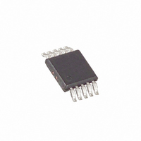
MAX4584EUB+ Maxim Integrated Products, MAX4584EUB+ Datasheet - Page 6

MAX4584EUB+
Manufacturer Part Number
MAX4584EUB+
Description
IC AUDIO/VIDEO SWITCH 10UMAX
Manufacturer
Maxim Integrated Products
Datasheet
1.MAX4584EUB.pdf
(12 pages)
Specifications of MAX4584EUB+
Function
Audio/Video Switch
Circuit
1 x SPST - NO, 1 x SPDT
On-state Resistance
65 Ohm
Voltage Supply Source
Single Supply
Voltage - Supply, Single/dual (±)
2.7 V ~ 5.5 V
Current - Supply
5µA
Operating Temperature
-40°C ~ 85°C
Mounting Type
Surface Mount
Package / Case
10-MSOP, Micro10™, 10-uMAX, 10-uSOP
Lead Free Status / RoHS Status
Lead free / RoHS Compliant
Serially Controlled
Audio/Video Switches
3-WIRE TIMING CHARACTERISTICS
(Figures 3 and 4, V+ = +2.75V to +5.25V, f
T
6
Note 2:
Note 3:
Note 4:
Note 5:
Note 6:
Note 7:
Note 8:
Note 9:
Note 10: C
Note 11: Typical values are for MAX4584 devices.
(V+ = +5V, T
A
Operating Frequency
DIN to SCLK Setup
DIN to SCLK Hold
CS Fall to SCLK Rise Setup
CS Rise to SCLK Hold
SCLK Pulse Width Low
SCLK Pulse Width High
Rise Time (SCLK, DIN, CS)
Fall Time (SCLK, DIN, CS)
CS Pulse Width High
= +25°C.)
_______________________________________________________________________________________
70
65
60
55
50
45
40
35
30
0
PARAMETER
Algebraic convention is used in this data sheet; the most negative value is shown in the minimum column.
Guaranteed by design. Not subject to production testing.
∆R
Resistance flatness is defined as the difference between the maximum and minimum on-resistance values, as measured
over the specified analog signal range.
Leakage parameters are 100% tested at maximum rated temperature and guaranteed by correlation at T
Off-isolation = 20 log (V
All timing is measured from the clock’s falling edge preceding the ACK signal for 2-wire and from the rising edge of CS for
3-wire. Turn-off time is defined at the output of the switch for a 0.5V change, tested with a 300Ω load to ground. Turn-on
time is defined at the output of the switch for a 0.5V change and measured with a 5kΩ load resistor to GND. All timing is
shown with respect to 20% V+ and 70% V+, unless otherwise noted.
Leakage testing is guaranteed by testing with a +5.25V supply.
vs. V
B
ON
A
1
= capacitance of one bus line in pF. Tested with C
= +25°C, unless otherwise noted.)
COM
= R
ON-RESISTANCE
AND SUPPLY VOLTAGE
2
ON(MAX)
V+ = 2.7V
V
COM
V+ = 3.0V
(V)
3
V+ = 5.5V
V+ = 4.0V
- R
4
ON(MIN)
V+ = 5.0V
COM
SYMBOL
5
t
t
t
CSW
_ / V
f
t
CSH
t
t
CSS
t
OP
DH
CH
DS
CL
t
t
.
R
F
NO
_ _), V
OP
V+ = 2.7V to 5.25V
V+ = 4.75V to 5.25V
55
50
45
40
35
30
= 2.1MHz, T
COM
0
vs. V
_ = output, V
COM
1
AND TEMPERATURE (V+ = 5V)
ON-RESISTANCE
CONDITIONS
T
A
B
T
A
A
= +125°C
2
= 400pF.
= T
= +25°C
V
COM
T
NO
A
MIN
(V)
T
= -55°C
Typical Operating Characteristics
A
_ _ = input to off switch.
3
= +85°C
to T
T
A
MAX
4
= -40°C
, unless otherwise noted. Typical values are at
5
75
70
65
60
55
50
45
40
35
30
vs. V
0
MIN
100
100
200
200
0
0
0
COM
0.5
AND TEMPERATURE (V+ = 3.3V)
TYP
ON-RESISTANCE
1.0
40
T
T
A
T
A
A
V
= +85 C
= -40 C
COM
= +25 C
1.5
A
(V)
MAX
= +25°C.
2.1
10
2
2
2.0
T
A
T
= -55 C
A
= +125 C
2.5
UNITS
MHz
ns
ns
ns
ns
ns
ns
µs
µs
ns
3.0


