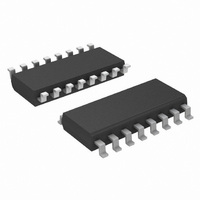
DG411DY-T1-E3 Vishay, DG411DY-T1-E3 Datasheet - Page 8

DG411DY-T1-E3
Manufacturer Part Number
DG411DY-T1-E3
Description
IC SWITCH QUAD SPST 16SOIC
Manufacturer
Vishay
Datasheet
1.DG411DY-T1-E3.pdf
(9 pages)
Specifications of DG411DY-T1-E3
Function
Switch
Circuit
4 x SPST - NC
On-state Resistance
45 Ohm
Voltage Supply Source
Single, Dual Supply
Voltage - Supply, Single/dual (±)
5 V ~ 44 V, ±5 V ~ 20 V
Current - Supply
-1µA, 1µA
Operating Temperature
-40°C ~ 85°C
Mounting Type
Surface Mount
Package / Case
16-SOIC (0.154", 3.90mm Width)
Number Of Switches
Quad
Switch Configuration
SPST
On Resistance (max)
80 Ohms
On Time (max)
250 ns
Off Time (max)
145 ns
Supply Voltage (max)
25 V
Supply Current
0.0000001 mA
Maximum Power Dissipation
600 mW
Maximum Operating Temperature
+ 85 C
Mounting Style
SMD/SMT
Minimum Operating Temperature
- 40 C
Analog Switch Type
SPST
No. Of Channels
4
On State Resistance Max
25ohm
Turn Off Time
100ns
Turn On Time
110ns
Supply Voltage Range
± 13.5V To ± 16.5V
Lead Free Status / RoHS Status
Lead free / RoHS Compliant
Lead Free Status / RoHS Status
Lead free / RoHS Compliant, Lead free / RoHS Compliant
Other names
DG411DY-T1-E3TR
Available stocks
Company
Part Number
Manufacturer
Quantity
Price
Company:
Part Number:
DG411DY-T1-E3
Manufacturer:
NXP
Quantity:
614
Part Number:
DG411DY-T1-E3
Manufacturer:
VISHAY/威世
Quantity:
20 000
DG411, DG412, DG413
Vishay Siliconix
APPLICATIONS
Single Supply Operation:
The DG411, DG412, DG413 can be operated with unipolar
supplies from 5 V to 44 V. These devices are characterized
and tested for unipolar supply operation at 12 V to facilitate
the majority of applications. In single supply operation, V+ is
tied to V
vs. Supply Voltage curve for V
requirments.
Vishay Siliconix maintains worldwide manufacturing capability. Products may be manufactured at one of several qualified locations. Reliability data for Silicon
Technology and Package Reliability represent a composite of all qualified locations. For related documents such as package/tape drawings, part marking, and
reliability data, see www.vishay.com/ppg?70050.
www.vishay.com
8
V
S
R
g
L
= 50 Ω
and V- is tied to 0 V. See Input Switching Threshold
0 V, 2.4 V
Figure 6. Off Isolation
V
V
IN 1
IN 2
C
S
IN
GND
Off Isolation = 20 log
+ 5 V
V
C = RF Bypass
L
L
+ 15 V
versus input threshold
- 15 V
DG413
V-
V+
D
C
V
V
S
O
C
Figure 8. Summing Amplifier
R
50 Ω
V
L
O
R
R
1
3
C
C
1
2
R
R
Summing Amplifier
When driving a high impedance, high capacitance load such
as shown in figure 8, where the inputs to the summing
amplifier have some noise filtering, it is necessary to have
shunt switches for rapid discharge of the filter capacitor, thus
preventing offsets from occurring at the output.
2
4
0 V, 2.4 V
R
C
6
IN
Figure 7. Source/Drain Capacitances
+ 5 V
GND
V
L
-
+
R
5
+ 15 V
- 15 V
V-
V+
S
D
S11-0179-Rev. F, 07-Feb-11
C
C
Document Number: 70050
V
OUT
or Equivalent
Impedance
HP4192A
Analyzer
Meter


