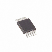
MAX4636EUB+ Maxim Integrated Products, MAX4636EUB+ Datasheet - Page 8

MAX4636EUB+
Manufacturer Part Number
MAX4636EUB+
Description
IC SWITCH DUAL SPDT 10UMAX
Manufacturer
Maxim Integrated Products
Datasheet
1.MAX4636EUB.pdf
(11 pages)
Specifications of MAX4636EUB+
Function
Switch
Circuit
2 x SPDT
On-state Resistance
4 Ohm
Voltage Supply Source
Single Supply
Voltage - Supply, Single/dual (±)
1.8 V ~ 5.5 V
Current - Supply
1µA
Operating Temperature
-40°C ~ 85°C
Mounting Type
Surface Mount
Package / Case
10-MSOP, Micro10™, 10-uMAX, 10-uSOP
Number Of Switches
Dual
Switch Configuration
SPDT
On Resistance (max)
4 Ohms
On Time (max)
14 ns
Off Time (max)
6 ns
Off Isolation (typ)
- 62 dB
Supply Voltage (max)
5.5 V
Supply Voltage (min)
1.8 V
Supply Current
0.001 uA
Maximum Power Dissipation
330 mW
Maximum Operating Temperature
+ 85 C
Mounting Style
SMD/SMT
Description/function
Analog Switch
Input Level
CMOS, TTL
Minimum Operating Temperature
- 40 C
Off State Leakage Current (max)
0.1 nA
Lead Free Status / RoHS Status
Lead free / RoHS Compliant
Fast, Low-Voltage, Dual 4
CMOS Analog Switches
The MAX4635/MAX4636 are low-on-resistance (R
low-voltage, dual SPDT analog switches that operate
from a +1.8V to +5.5V supply. The MAX4635/MAX4636
feature very fast switching speed (t
t
switching. The low maximum R
ous currents to be switched in a variety of applications.
Figure 3. Channel Off/On-Capacitance
Figure 4. On-Loss, Off-Isolation, and Crosstalk
8
OFF
_______________________________________________________________________________________
CAPACITANCE
= 6ns max) and guaranteed break-before-make
f = 1MHz
METER
MEASUREMENTS ARE STANDARDIZED AGAINST SHORTS AT IC TERMINALS.
OFF-ISOLATION IS MEASURED BETWEEN COM_ AND "OFF" NO_ OR NC_ TERMINAL ON EACH SWITCH.
ON-LOSS IS MEASURED BETWEEN COM_ AND "ON" NO_ OR NC_ TERMINAL ON EACH SWITCH.
CROSSTALK IS MEASURED FROM ONE CHANNEL TO ALL OTHER CHANNELS.
SIGNAL DIRECTION THROUGH SWITCH IS REVERSED; WORST VALUES ARE RECORDED.
50
0 OR V+
Applications Information
IN_
NC_
Detailed Description
10nF
COM_
NC_ OR
NO_
MAX4635
MAX4636
GND
+5V
GND
V+
V+
V+
ON
10nF
COM_
MAX4635
MAX4636
NO_
allows high continu-
ON
IN_
= 14ns max,
V
V
IN
OUT
V
V
OR
INL
INH
ON
),
MEAS
50
50
The MAX4635/MAX4636 logic inputs (IN1, IN2) can be
driven up to +5.5V, regardless of the voltage on V+.
This allows interfacing to 5V logic signals while operat-
ing with a +3.3V supply voltage without external level
translation.
Analog signals ranging over the entire supply voltage
(V+ to GND) can be passed with very little change in
on-resistance (see Typical Operating Characteristics).
The switches are bidirectional, so the NO_, NC_, and
COM_ pins may be used as either inputs or outputs.
Caution: Do not exceed the absolute maximum rat-
ings because stresses beyond the listed ratings can
cause permanent damage to the device. Proper
power-supply sequencing is recommended for all
CMOS devices. Always apply V+ before applying ana-
log signals, especially if the analog signal is not current
limited. If this sequencing is not possible, and if the
analog inputs are not current limited to less than 30mA,
add a small-signal diode (D1) as shown in Figure 5. If
the analog signal can dip below GND, add D2. Adding
protection diodes reduces the analog range to a diode
drop (about 0.7V) below V+ (for D1), and a diode drop
above ground (for D2).
ANALYZER
NETWORK
SPDT
50
50
REF
Power-Supply Sequencing and
Overvoltage Protection
OFF-ISOLATION = 20log
Analog Signal Levels
CROSSTALK = 20log
ON-LOSS = 20log
Logic Inputs
V
V
V
V
V
V
OUT
OUT
OUT
IN
IN
IN


