LMH6586VS/NOPB National Semiconductor, LMH6586VS/NOPB Datasheet
LMH6586VS/NOPB
Specifications of LMH6586VS/NOPB
LMH6586VS
Available stocks


Related parts for LMH6586VS/NOPB

LMH6586VS/NOPB Summary of contents
Page 1
... The LMH6586 operates from a common single 5V supply for its analog sections as well as its control logic and interface. The LMH6586 is offered in a space-saving 80-pin TQFP. LMH™ trademark of National Semiconductor Corporation. © 2008 National Semiconductor Corporation Features ■ 32 inputs and 16 outputs ■ ...
Page 2
Application Diagram www.national.com 2 30056946 ...
Page 3
Functional Diagram FIGURE 1. Functional Diagram 3 30056902 www.national.com ...
Page 4
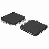
Connection Diagram Ordering Information Package Part Number 80-Pin TQFP LMH6586VS www.national.com Package Marking Transport Media LMH6586VS 119 Units/Tray 4 30056901 NSC Drawing VHB80A ...
Page 5
Pin Descriptions Pin # Pin Name 1 VIN_31 2 VIN_30 3 VIN_29 4 VIN_28 5 VIN_27 6 VIN-26 7 VIN_25 8 VIN_24 9 VDD 10 GND 11 VIN_23 12 VIN_22 13 VIN_21 14 VIN_20 15 VIN_19 16 VIN_18 17 VIN_17 ...
Page 6
Pin # Pin Name 49 VIN_6 50 VIN_7 51 GND 52 VDD 53 VIN_8 54 VIN_9 55 VIN_10 56 VIN_11 57 VIN_12 58 VIN_13 59 VIN_14 60 VIN_15 61 GAIN 62 VDD 63 GND 64 VBIAS 2 65 VREF_SYNC 66 ...
Page 7
... Absolute Maximum Ratings If Military/Aerospace specified devices are required, please contact the National Semiconductor Sales Office/ Distributors for availability and specifications. ESD Tolerance (Note 2) Human Body Model Machine Model Supply Voltage ( Video Input Voltage Range Electrical Characteristics = 10 kΩ 1%, VREF_CLAMP = 300 mV EXT ...
Page 8
FIGURE 2. Logic Diagram 8 30056944 ...
Page 9
Typical Performance Characteristics = 10 kΩ 1 150Ω pF. Small Signal Input Signal = 20 mV EXT L L Signal Input Signal = 750 mV PP Small Signal Bandwidth Medium Signal Bandwidth Large Signal ...
Page 10
Small Signal Gain Flatness Small Signal Gain Peaking Large Signal Gain Flatness www.national.com Small Signal Gain Flatness 30056912 Small Signal Gain Peaking 30056914 Large Signal Gain Flatness 30056916 10 30056913 30056915 30056917 ...
Page 11
Large Signal Gain Peaking 30056918 Adjacent Channel Crosstalk 30056920 All Hostile Crosstalk 30056922 Large Signal Gain Peaking Adjacent Channel Crosstalk All Hostile Crosstalk 11 30056919 30056921 30056923 www.national.com ...
Page 12
Off Isolation Small Signal Pulse Response Small Signal Pulse Response www.national.com Small Signal Pulse Response 30056924 Small Signal Pulse Response 30056926 Small Signal Pulse Response with Capacitive Load 30056928 12 30056925 30056927 30056929 ...
Page 13
Small Signal Pulse Response with Capacitive Load Medium Signal Pulse Response Medium Signal Pulse Response Medium Signal Pulse Response 30056930 Medium Signal Pulse Response 30056932 Medium Signal Pulse Response with Capacitive Load 30056934 13 30056931 30056933 30056935 www.national.com ...
Page 14
Medium Signal Pulse Response with Capacitive Load Large Signal Pulse Response Large Signal Pulse Response www.national.com Large Signal Pulse Response 30056936 Large Signal Pulse Response 30056938 Large Signal Pulse Response with Capacitive Load 30056940 14 30056937 30056939 30056941 ...
Page 15
Large Signal Pulse Response with Capacitive Load Differential Phase 0.6V Output Level = 0 IRE 1.3V Output Level = 100 IRE Differential Phase 0.6V Output Level = 0 IRE 1.3V Output Level = 100 IRE Differential Phase 30056942 0.6V Output ...
Page 16
Differential Gain 0.6V Output Level = 0 IRE 1.3V Output Level = 100 IRE Differential Gain 0.6V Output Level = 0 IRE 1.3V Output Level = 100 IRE Harmonic Distortion www.national.com Differential Gain 30056952 0.6V Output Level = 0 IRE ...
Page 17
Application Information FUNCTIONAL OVERVIEW The LMH6586 is a non-blocking analog video crosspoint switch with 32 input channels and 16 output channels. The inputs have integrated DC restore clamp circuits for biasing the AC-coupled video inputs. The fully buffered outputs have ...
Page 18
The switch can only be configured by programming through the I DC RESTORATION Because the LMH6586 uses a single 5V ...
Page 19
When shutdown the outputs are high impedance, which re- duces power consumption and crosstalk, and also enables multiple outputs to be connected together for expanding the matrix array size. Note that output short circuit protection is not provided, so care ...
Page 20
LMH6586VS 80-Pin TQFT LMHXPT Analog Video Crosspoint Board NO Heat Sink Small Tower 9.57x9.69 mm/ht. 6.28 mm Aluminum 12 rail 9.82x10.73 mm/ht.10.07 mm Anodized 9 rail 6.10x7.30 mm/ht. 13.67 mm Round ...
Page 21
READ SEQUENCE Read sequences are comprised of two I The first is the address access transfer, which consists of a write sequence that transfers only the address to be ac- cessed. The second is the data read transfer, which starts ...
Page 22
REGISTER DESCRIPTIONS Video and Sync Detection Status Registers Registers 0x00 to 0x03 (read-only) contain the sync detection status bits for all 32 input channels. Any input (m) has a sync detection status bit (SD_m) that can flag high when a ...
Page 23
TABLE 3. Video and Sync Detection Control Registers Register Address R/W RESERVED 0x08h R/W 0x0Bh VIDEO DETECT 0x0Ch R/W INVERT (CH 0-7) VIDEO DETECT 0x0Dh R/W INVERT (CH 8-15) VIDEO DETECT 0x0Eh R/W INVERT (CH 16-23) VIDEO DETECT 0x0Fh R/W ...
Page 24
Register Address CH 0 OUTPUT 0x20h CH 1 OUTPUT 0x21h CH 2 OUTPUT 0x22h CH 3 OUTPUT 0x23h CH 4 OUTPUT 0x24h CH 5 OUTPUT 0x25h CH 6 OUTPUT 0x26h CH 7 OUTPUT 0x27h CH 8 OUTPUT 0x28h CH 9 ...
Page 25
Physical Dimensions inches (millimeters) unless otherwise noted 80-Pin TQFP NS Package Number VHB80A 25 www.national.com ...
Page 26
... For more National Semiconductor product information and proven design tools, visit the following Web sites at: Products Amplifiers www.national.com/amplifiers Audio www.national.com/audio Clock and Timing www.national.com/timing Data Converters www.national.com/adc Interface www.national.com/interface LVDS www.national.com/lvds Power Management www.national.com/power Switching Regulators www.national.com/switchers LDOs www.national.com/ldo LED Lighting www ...