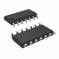
LMH6574MA/NOPB National Semiconductor, LMH6574MA/NOPB Datasheet - Page 2

LMH6574MA/NOPB
Manufacturer Part Number
LMH6574MA/NOPB
Description
IC VIDEO MULTIPLEXER 4X1 14SOIC
Manufacturer
National Semiconductor
Datasheet
1.LMH6574MANOPB.pdf
(14 pages)
Specifications of LMH6574MA/NOPB
Function
Video Multiplexer
Circuit
1 x 4:1
Voltage Supply Source
Single, Dual Supply
Voltage - Supply, Single/dual (±)
6 V ~ 12 V, ±3 V ~ 6 V
Current - Supply
13mA
Operating Temperature
-40°C ~ 85°C
Mounting Type
Surface Mount
Package / Case
14-SOIC (0.154", 3.90mm Width)
For Use With
LMH730276 - EVAL BOARD FOR HS 4:1 MUX
Lead Free Status / RoHS Status
Lead free / RoHS Compliant
Other names
*LMH6574MA
*LMH6574MA/NOPB
LMH6574MA
*LMH6574MA/NOPB
LMH6574MA
www.national.com
Frequency Domain Performance
SSBW
LSBW
.1 dBBW
DG
DP
XTLK
Time Domain Response
TRS
TRL
TSS
OS
SR
Distortion
HD2
HD3
IMD
Equivalent Input Noise
VN
ICN
Static, DC Performance
CHGM
VIO
DVIO
IBN
DIBN
PSRR
Symbol
Absolute Maximum Ratings
If Military/Aerospace specified devices are required,
please contact the National Semiconductor Sales Office/
Distributors for availability and specifications.
V
perature extremes.
±
S
ESD Tolerance
Supply Voltage (V
I
Signal & Logic Input Pin Voltage
Signal & Logic Input Pin Current
Maximum Junction Temperature
5V Electrical Characteristics
OUT
=
Human Body Model
Machine Model
±
5V, R
(Note 3)
−3 dB Bandwidth
–3 dB Bandwidth
0. 1 dB Bandwidth
Differential Gain
Differential Phase
Channel to Channel Crosstalk
Channel to Channel Switching Time Logic Transition to 90% Output
Enable and Disable Times
Rise and Fall Time
Settling Time to 0.05%
Overshoot
Slew Rate
2
3
3
Voltage
Current
Channel to Channel Gain
Difference
Input Offset Voltage (Note 5)
Input Bias Current (Notes 7, 5)
Inverting Input Bias Current
Power Supply Rejection Ratio
(Note 5)
nd
rd
rd
Bias Current Drift
Offset Voltage Drift
L
Harmonic Distortion
Order Intermodulation Products
Harmonic Distortion
= 100Ω, A
+
− V
Parameter
V
−
)
= 2 V/V, R
F
= 575 Ω, T
±
(Note 1)
(V
V
V
V
R
R
All Hostile, 5 MHz
Logic Transition to 90% or 10%
Output
4V Step
2V Step
2V Step
4V Step
2 V
2 V
10 MHz, Two Tones 2 V
Output
>
>
DC, Difference in Gain Between
Channels
V
V
Pin 12, Feedback Point,
V
DC, Input Referred
(Note 4)
±
OUT
OUT
OUT
IN
IN
IN
L
L
130 mA
S
1 MHz, Input Referred
1 MHz, Input Referred
+150˚C
J
+0.6V)
20 mA
2000V
= 150Ω, f = 4.43 MHz
= 150Ω, f = 4.43MHz
PP
PP
13.2V
= 0V
= 0V
= 0V
= 25 ˚C, Unless otherwise specified. Bold numbers specify limits at tem-
200V
= 0.5 V
= 2 V
= 0.25 V
, 5 MHz
, 5 MHz
Conditions (Note 2)
PP
PP
PP
2
Operating Ratings
Operating Temperature
Supply Voltage Range
Package
14-Pin SOIC
Storage Temperature Range
Soldering Information
Thermal Resistance
Infrared or Convection (20 sec)
Wave Soldering (10 sec)
PP
at
Min
47
45
±
2200
0.02
0.05
Typ
−85
−68
−84
−80
0.005
500
400
150
2.4
−3
−7
(Note 1)
10
17
30
11
54
8
5
5
5
1
−40 ˚C to 85 ˚C
6V to 12V
(θ
130˚C/W
JA
)
−65˚C to +150˚C
±
±
±
Max
0.032
0.035
±
±
±
±
±
5.6
20
25
10
13
5
40˚C/W
235 ˚C
260 ˚C
pA/
nV
(θ
Units
µV/˚C
nA/˚C
MHz
MHz
MHz
V/µs
dBc
dBc
dBc
deg
JC
mV
dB
µA
dB
ns
ns
ns
ns
%
%
%
)


