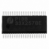
PI3B33X257BE Pericom Semiconductor, PI3B33X257BE Datasheet - Page 2

PI3B33X257BE
Manufacturer Part Number
PI3B33X257BE
Description
IC MUX/DEMUX QUAD 1X2 48BQSOP
Manufacturer
Pericom Semiconductor
Datasheet
1.PI3B33X257BE.pdf
(4 pages)
Specifications of PI3B33X257BE
Function
Multiplexer/Demultiplexer
Circuit
4 x 1:2
On-state Resistance
15 Ohm
Current - Supply
9µA
Operating Temperature
-40°C ~ 85°C
Mounting Type
Surface Mount
Package / Case
48-BQSOP
Configuration
4 x 2:1
Number Of Inputs
24
Number Of Outputs
12
Operating Supply Voltage (typ)
3.3V
Operating Supply Voltage (min)
3.135V
Operating Supply Voltage (max)
3.465V
Power Dissipation
500mW
Operating Temp Range
-40C to 85C
Operating Temperature Classification
Industrial
Mounting
Surface Mount
Pin Count
48
Package Type
BQSOP
Lead Free Status / RoHS Status
Lead free / RoHS Compliant
Available stocks
Company
Part Number
Manufacturer
Quantity
Price
Pin Description
Maximum Ratings
(Above which the useful life may be impaired. For user guidelines, not tested.)
DC Electrical Characteristics
Parameters
V
V
I
I
I
V
R
Storage Temperature ............................................................ –65°C to +150°C
Ambient Temperature with Power Applied ........................... –40°C to +85°C
Supply Voltage to Ground Potential .......................................–0.5V to +4.6V
DC Input Voltage ....................................................................–0.5V to +4.6V
DC Output Current............................................................................... 120mA
Power Dissipation ................................................................................... 0.5W
IH
IL
OZH
ON
IH
IL
IK
IA
S
En
Y
GND
V
NC
A
CC
n
-Y
-IL
L
n
Pin Name
Description
Input HIGH Voltage
Input LOW Voltage
Input HIGH Current
Input LOW Current
High Impedance Output
Current
Clamp Diode Voltage
Switch On-Resistance
Data Inputs
Select Inputs
Enable
Data Outputs
Ground
Power
No Connect
(Over the Operating Range, T
(3)
Description
Test Conditions
Guaranteed Logic HIGH Level
Guaranteed Logic LOW Level
V
V
0 ≤ I, Y ≤ V
V
V
V
CC
CC
CC
CC
CC
= Max., V
= Max., V
= Min., I
= Min., V
= Min., V
CC
IN
IN
IN
IN
IN
(1)
= –18mA
= 0.0V, I
= 2.4V, I
= GND
= V
2
A
Truth Table
Notes:
1.
2.
CC
= –40°C to +85°C, V
En
H
L
L
H = High Voltage Level,
L = Low Voltage Level
n = 0 YA, YB, YC, YD,
n = 1 YE, YF, YG, YH,
n = 2 YI, YJ, YK, YL
ON
ON
= 48mA or 64mA
= 15mA
Sn
X
H
L
Note:
Stresses greater than those listed under MAXIMUM RAT-
INGS may cause permanent damage to the device. This is
a stress rating only and functional operation of the device
at these or any other conditions above those indicated in
the operational sections of this specification is not implied.
Exposure to absolute maximum rating conditions for ex-
tended periods may affect reliability.
(1)
3.3V, 24:12 Mux/DeMux NanoSwitch
YA
Hi-Z
I
I
A
A
(2)
0
1
CC
YB
Hi-Z
= 3.3V ±5%)
I
I
B
B
(2)
0
1
–0.5
Min.
2.0
YC
Hi-Z
I
I
C
C
(2)
0
1
Typ.
10
YD
5
Hi-Z
I
I
(2)
D
D
PS8334D
(2)
0
1
PI3B33X257
Max.
–1.2
±50
±50
0.8
±1
15
7
Function
Disable
S = 0
S = 1
Units
11/01/04
µA
V
V
Ω
™


