ADG529AKNZ Analog Devices Inc, ADG529AKNZ Datasheet - Page 5
ADG529AKNZ
Manufacturer Part Number
ADG529AKNZ
Description
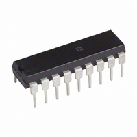
IC MULTIPLEXER DUAL 4X1 18DIP
Manufacturer
Analog Devices Inc
Datasheet
1.ADG529AKNZ.pdf
(12 pages)
Specifications of ADG529AKNZ
Function
Multiplexer
Circuit
2 x 4:1
On-state Resistance
300 Ohm
Voltage Supply Source
Dual Supply
Voltage - Supply, Single/dual (±)
±10.8 V ~ 16.5 V
Current - Supply
20µA
Operating Temperature
-40°C ~ 85°C
Mounting Type
Through Hole
Package / Case
18-DIP (0.300", 7.62mm)
No. Of Circuits
2
Supply Current
600µA
On State Resistance Max
500ohm
Supply Voltage Range
10.8V To 16.5V
Operating Temperature Range
-40°C To +85°C
Analog Switch Case Style
DIP
Lead Free Status / RoHS Status
Lead free / RoHS Compliant
Available stocks
Company
Part Number
Manufacturer
Quantity
Price

Part Number:
ADG529AKNZ
Manufacturer:
ADI/亚德诺
Quantity:
20 000


CAUTION
ESD (electrostatic discharge) sensitive device. Electrostatic charges as high as 4000 V readily
accumulate on the human body and test equipment and can discharge without detection. Although the
ADG528A/ADG529A features proprietary ESD protection circuitry, permanent damage may occur
on devices subjected to high energy electrostatic discharges. Therefore, proper ESD precautions are
recommended to avoid performance degradation or loss of functionality.
REV. B
DIP/SOIC
PIN CONFIGURATIONS
Model
ADG528AKN
ADG528AKP
ADG528AKP-REEL
ADG528ABQ
ADG528ATQ
ADG528ABCHIPS
ADG528ATCHIPS
ADG529AKN
ADG529AKP
ADG529AKRW
ADG529AKRW-REEL
ADG529AKRW-REEL7
ADG529ABQ
ADG529ATQ
ADG529ABCHIPS
ADG529ATCHIPS
NOTES
1
N = Plastic DIP; P = Plastic Leaded Chip Carrier (PLCC); Q = Cerdip; RW = SOIC.
PLCC
Temperature
Range
–40°C to +85°C
–40°C to +85°C
–40°C to +85°C
–40°C to +85°C
–55°C to +125°C
–40°C to +85°C
–40°C to +85°C
–40°C to +85°C
–40°C to +85°C
–40°C to +85°C
–40°C to +85°C
–55°C to +125°C
ORDERING GUIDE
–5–
ABSOLUTE MAXIMUM RATINGS
(T
V
V
V
Analog Inputs
Digital Inputs
Power Dissipation (Any Package)
Operating Temperature
Storage Temperature Range . . . . . . . . . . . . . –65°C to +150°C
Lead Temperature (Soldering, 10 sec) . . . . . . . . . . . . +300°C
NOTES
1
2
Stresses above those listed under “Absolute Maximum Ratings” may cause permanent
damage to the device. This is a stress rating only and functional operation of the device
at these or any other conditions above those indicated in the operational sections of this
specification is not implied. Exposure to absolute maximum rating conditions for
extended periods may affect device reliability.
Overvoltage at A, EN, WR, RS, S or D will be clamped by diodes. Current should
be limited to the maximum rating above.
DD
DD
SS
Voltage at S, D . . . . . . . . . V
Continuous Current, S or D . . . . . . . . . . . . . . . . . . . 20 mA
Pulsed Current, S or D
Voltage at A, EN, WR, RS . . . . . . V
Up to +75°C . . . . . . . . . . . . . . . . . . . . . . . . . . . . . . 470 mW
Derates above +75°C . . . . . . . . . . . . . . . . . . . . . . . 6 mW/°C
Commercial (K Version) . . . . . . . . . . . . . . . –40°C to +85°C
Industrial (B Version) . . . . . . . . . . . . . . . . . –40°C to +85°C
Extended (T Version) . . . . . . . . . . . . . . . . –55°C to +125°C
A
to GND . . . . . . . . . . . . . . . . . . . . . . . . . . . . . . . . . . . –25 V
= +25°C, unless otherwise noted)
1 ms duration, 10% Duty Cycle . . . . . . . . . . . . . . . 40 mA
to V
to GND . . . . . . . . . . . . . . . . . . . . . . . . . . . . . . . . . . . 25 V
SS
Package
Description
PDIP
PLCC
PLCC
CERDIP
CERDIP
DIE
DIE
PDIP
PLCC
SOIC
SOIC
SOIC
CERDIP
CERDIP
DIE
DIE
. . . . . . . . . . . . . . . . . . . . . . . . . . . . . . . . . . . . . 44 V
1
2
Package
Option
N-18
P-20A
P-20A
Q-18
Q-18
N-18
P-20A
RW-18
RW-18
RW-18
Q-18
Q-18
ADG528A/ADG529A
SS
20 mA, whichever Occurs First
WARNING!
– 2 V to V
1
1
SS
whichever Occurs First
– 4 V to V
ESD SENSITIVE DEVICE
DD
+ 2 V or 20 mA,
DD
+ 4 V or
Related parts for ADG529AKNZ
Image
Part Number
Description
Manufacturer
Datasheet
Request
R

Part Number:
Description:
±1.7g Dual-Axis IMEMS Accelerometer Evaluation Board
Manufacturer:
Analog Devices Inc
Datasheet:

Part Number:
Description:
Inertial Sensor Evaluation System
Manufacturer:
Analog Devices Inc
Datasheet:
Part Number:
Description:
Manufacturer:
Analog Devices Inc
Datasheet:
Part Number:
Description:
Manufacturer:
Analog Devices Inc
Datasheet:
Part Number:
Description:
Manufacturer:
Analog Devices Inc
Datasheet:
Part Number:
Description:
Manufacturer:
Analog Devices Inc
Datasheet:
Part Number:
Description:
Manufacturer:
Analog Devices Inc
Datasheet:
Part Number:
Description:
Manufacturer:
Analog Devices Inc
Datasheet:
Part Number:
Description:
Manufacturer:
Analog Devices Inc
Datasheet:
Part Number:
Description:
Manufacturer:
Analog Devices Inc
Datasheet:
Part Number:
Description:
Manufacturer:
Analog Devices Inc
Datasheet:
Part Number:
Description:
Manufacturer:
Analog Devices Inc
Datasheet:
Part Number:
Description:
Manufacturer:
Analog Devices Inc
Datasheet: