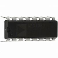
ADG408BNZ Analog Devices Inc, ADG408BNZ Datasheet - Page 13

ADG408BNZ
Manufacturer Part Number
ADG408BNZ
Description
IC MULTIPLEXER 8X1 16DIP
Manufacturer
Analog Devices Inc
Series
LC²MOSr
Type
Analog Multiplexerr
Specifications of ADG408BNZ
Function
Multiplexer
Circuit
1 x 8:1
On-state Resistance
100 Ohm
Voltage Supply Source
Single Supply
Voltage - Supply, Single/dual (±)
5V, 12V
Current - Supply
100µA
Operating Temperature
-40°C ~ 85°C
Mounting Type
Through Hole
Package / Case
16-DIP (0.300", 7.62mm)
No. Of Circuits
1
Supply Current
100µA
On State Resistance Max
40ohm
Supply Voltage Range
12V, ± 15V
Operating Temperature Range
-40°C To +85°C
Analog Switch Case Style
DIP
No. Of Pins
16
Multiplexer Configuration
Single 8:1
Number Of Inputs
8
Number Of Outputs
1
Number Of Channels
1
Analog Switch On Resistance
100@±15VOhm
Analog Switch Turn On Time
150ns
Analog Switch Turn Off Time
60ns
Package Type
PDIP
Power Supply Requirement
Single/Dual
Single Supply Voltage (min)
5V
Single Supply Voltage (typ)
12V
Single Supply Voltage (max)
12V
Dual Supply Voltage (typ)
±15V
Dual Supply Voltage (max)
±22V
Power Dissipation
470mW
Mounting
Through Hole
Pin Count
16
Operating Temp Range
-40C to 85C
Operating Temperature Classification
Industrial
Amplifier Type
Analog Multiplexer
Capacitance, Drain Off
40 pF (Typ.)
Capacitance, Drain On
54 pF (Typ.)
Capacitance, Source Off
11 pF (Typ.)
Current, Leakage, Drain-off
±1 nA (Max.) @ +25 °C
Current, Leakage, Drain-on
±1 nA (Max.) @ +25 °C
Resistance, Drain To Source On
40 Ohms (Typ.) @ +25 °C
Temperature, Operating, Maximum
85 °C
Temperature, Operating, Minimum
-40 °C
Time, Transistion
120 ns (Typ.)
Time, Turn-off Enable
65 ns (Typ.)
Time, Turn-on Enable
125 ns (Typ.)
Voltage, Input, Logic High
2.4 V (Min.)
Voltage, Supply
44 V (Max.)
Lead Free Status / RoHS Status
Lead free / RoHS Compliant
Lead Free Status / RoHS Status
Lead free / RoHS Compliant, Lead free / RoHS Compliant
Available stocks
Company
Part Number
Manufacturer
Quantity
Price
Company:
Part Number:
ADG408BNZ
Manufacturer:
MOTOROLA
Quantity:
6 218
Part Number:
ADG408BNZ
Manufacturer:
ADI/亚德诺
Quantity:
20 000
TERMINOLOGY
R
Ohmic resistance between D and S.
ΔR
Difference between the R
I
Source leakage current when the switch is off.
I
Drain leakage current when the switch is off.
I
Channel leakage current when the switch is on.
V
Analog voltage on Terminal D and Terminal S.
C
Channel input capacitance for off condition.
C
Channel output capacitance for off condition.
C
On switch capacitance.
C
Digital input capacitance.
t
Delay time between the 50% and 90% points of the digital input
and switch on condition.
t
Delay time between the 50% and 90% points of the digital input
and switch off condition.
ON
OFF
S
D
D
ON
S
D
D
IN
D
, I
(OFF)
(OFF)
, C
(OFF)
ON
(V
(OFF)
(EN)
S
(EN)
(ON)
S
S
)
(ON)
ON
of any two channels.
Rev. C | Page 13 of 16
t
Delay time between the 50% and 90% points of the digital
inputs and the switch on condition when switching from one
address state to another.
t
Off time measured between the 80% point of both switches
when switching from one address state to another.
V
Maximum input voltage for Logic 0.
V
Minimum input voltage for Logic 1.
I
Input current of the digital input.
Crosstalk
A measure of unwanted signal that is coupled through from one
channel to another as a result of parasitic capacitance.
Off Isolation
A measure of unwanted signal coupling through an off channel.
Charge Injection
A measure of the glitch impulse transferred from the digital
input to the analog output during switching.
I
Positive supply current.
I
Negative supply current.
TRANSITION
OPEN
INL
DD
SS
INL
INH
(I
INH
)
ADG408/ADG409


