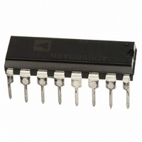
ADG509AKNZ Analog Devices Inc, ADG509AKNZ Datasheet - Page 5

ADG509AKNZ
Manufacturer Part Number
ADG509AKNZ
Description
IC MULTIPLEXER DUAL 4X1 16DIP
Manufacturer
Analog Devices Inc
Specifications of ADG509AKNZ
Function
Multiplexer
Circuit
2 x 4:1
On-state Resistance
300 Ohm
Voltage Supply Source
Dual Supply
Voltage - Supply, Single/dual (±)
±10.8 V ~ 16.5 V
Current - Supply
20µA
Operating Temperature
-40°C ~ 85°C
Mounting Type
Through Hole
Package / Case
16-DIP (0.300", 7.62mm)
No. Of Circuits
2
Supply Current
600µA
On State Resistance Max
280ohm
Supply Voltage Range
10.8V To 16.5V
Operating Temperature Range
-40°C To +85°C
Analog Switch Case Style
DIP
Lead Free Status / RoHS Status
Lead free / RoHS Compliant
Lead Free Status / RoHS Status
Lead free / RoHS Compliant, Lead free / RoHS Compliant
Available stocks
Company
Part Number
Manufacturer
Quantity
Price
Company:
Part Number:
ADG509AKNZ
Manufacturer:
ADI
Quantity:
36
Part Number:
ADG509AKNZ
Manufacturer:
ADI/亚德诺
Quantity:
20 000
SINGLE SUPPLY
V
Table 2.
Parameter
ANALOG SWITCH
DIGITAL CONTROL
DYNAMIC CHARACTERISTICS
POWER SUPPLY
1
Sample tested at 25°C to ensure compliance.
DD
Analog Signal Range
R
R
R
I
I
I
I
Leakage (ADG509A only)
V
V
I
C
t
t
t
t
OFF Isolation
C
C
Q
I
Power Dissipation
S
D
D
DIFF
INL
DD
TRANSITION
OPEN
ON
OFF
ON
ON
ON
ADG508A
ADG509A
ADG508A
ADG509A
INH
INL
IN
S
D
ADG508A
ADG509A
(OFF), Off Input Leakage
INJ
= 10.8 V to 16.5 V, V
(OFF), Off Output Leakage
(ON), On Channel Leakage
(OFF)
(OFF)
or I
, Differential Off Output
, Input Low Voltage
Digital Input Capacitance
(EN)
, Charge Injection
, Input High Voltage
(EN)
Drift
Match
1
INH
1
1
1
SS
= GND = 0 V, unless otherwise noted.
+25°C
GND
1
1
1
1
22
11
V
500
700
0.6
5
0.02
1
0.04
0.04
8
300
450
50
25
250
450
250
450
68
50
5
4
0.6
10
DD
ADG508A
ADG509A
K Version
–40°C to
+85°C
GND
V
1000
50
100
50
100
50
25
2.4
0.8
1
600
10
600
600
1.5
25
DD
+25°C
GND
V
500
700
0.6
5
0.02
1
0.04
1
1
0.04
1
1
8
300
450
50
25
250
450
250
450
68
50
5
22
11
4
0.6
10
DD
ADG508A
ADG509A
B Version
Rev. C | Page 5 of 16
–40°C to
+85°C
GND
V
1000
50
100
50
100
50
25
2.4
0.8
1
600
10
600
600
1.5
25
DD
+25°C
GND
V
500
700
0.6
5
0.02
1
0.04
1
1
0.04
1
1
8
300
450
50
25
250
450
250
450
68
50
5
22
11
4
0.6
10
DD
ADG508A
ADG509A
T Version
–55°C to
+125°C
GND
V
1000
50
100
50
100
50
25
2.4
0.8
1
600
10
600
600
1.5
25
DD
Unit
V min
V max
Ω typ
Ω max
nA typ
nA max
nA typ
nA max
nA max
nA max
nA max
nA max
V min
V max
μA max
pF max
ns typ
ns max
ns typ
ns min
ns typ
ns max
ns typ
ns max
dB typ
dB min
pF typ
pF typ
mA max
mW typ
mW max
%/°C typ
% typ
nA typ
pF typ
pC typ
mA typ
Comments
GND ≤ V
see
V
GND ≤ V
V1 = +10 V/GND, V2 = GND/+10 V;
see
V1 = +10 V/GND, V2 = GND/+10 V
See
V1 = V2 = +10 V/GND; see
V1 = +10 V/GND, V2 = GND/+10 V;
see
V
V1 = +10 V/GND, V2 = GND/+10 V;
see
See
See
See
V
V
V
V
R
V
EN
S
S
IN
S
EN
EN
IN
ADG508A/ADG509A
= 0, I
= 3.5 V rms, f = 100 kHz
= 0 Ω, V
= 0 to V
= V
= 0.8 V, R
= 0.8 V
= 0.8 V
Figure 14
Figure 15
Figure 18
Figure 19
Figure 16
Figure 20
Figure 21
Figure 21
INL
DS
S
S
or V
= 0.5 mA
≤ +10 V, I
≤ +10 V, I
S
DD
= 0 V; see
L
= 1kΩ, C
INH
DS
DS
L
= 0.5 mA;
= 0.5 mA
Figure 22
= 15 pF,
Figure 17


