DG9424DQ-T1-E3 Vishay, DG9424DQ-T1-E3 Datasheet - Page 6
DG9424DQ-T1-E3
Manufacturer Part Number
DG9424DQ-T1-E3
Description
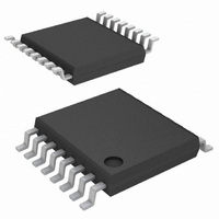
IC SWITCH QUAD SPST 16TSSOP
Manufacturer
Vishay
Datasheet
1.DG9424DQ-T1-E3.pdf
(11 pages)
Specifications of DG9424DQ-T1-E3
Function
Switch
Circuit
4 x SPST - NC
On-state Resistance
4 Ohm
Voltage Supply Source
Single, Dual Supply
Voltage - Supply, Single/dual (±)
2.7 V ~ 12 V, ± 3 V ~ 6 V
Current - Supply
5µA
Operating Temperature
-40°C ~ 85°C
Mounting Type
Surface Mount
Package / Case
16-TSSOP
Number Of Switches
Quad
Switch Configuration
SPST
On Resistance (max)
13.8 Ohms
On Time (max)
163 ns
Off Time (max)
80 ns
Off Isolation (typ)
- 56 dB
Supply Voltage (max)
12 V
Supply Voltage (min)
2.7 V
Supply Current
0.00002 mA
Maximum Power Dissipation
450 mW
Maximum Operating Temperature
+ 85 C
Mounting Style
SMD/SMT
Minimum Operating Temperature
- 40 C
Off State Leakage Current (max)
10 nA
Analog Switch Type
SPST
No. Of Channels
4
On State Resistance Max
1.8ohm
Turn Off Time
42ns
Turn On Time
56ns
Supply Voltage Range
2.7V To 12V
Operating Temperature Range
-40°C To +85°C
Lead Free Status / RoHS Status
Lead free / RoHS Compliant
Lead Free Status / RoHS Status
Lead free / RoHS Compliant, Lead free / RoHS Compliant
Other names
DG9424DQ-T1-E3TR
Available stocks
Company
Part Number
Manufacturer
Quantity
Price
Company:

Part Number:
DG9424DQ-T1-E3
Manufacturer:
Exar
Quantity:
2 107
Part Number:
DG9424DQ-T1-E3
Manufacturer:
VISHAY/威世
Quantity:
20 000


DG9424, DG9425, DG9426
Vishay Siliconix
Notes:
a. Leakage parameters are guaranteed by worst case test conditions and not subject to production test.
b. Room = 25 °C, Full = as determined by the operating temperature suffix.
c. Typical values are for DESIGN AID ONLY, not guaranteed nor subject to production testing.
d. The algebraic convention whereby the most negative value is a minimum and the most positive a maximum, is used in this data sheet.
e. Guaranteed by design, not subject to production test.
f. V
Stresses beyond those listed under “Absolute Maximum Ratings” may cause permanent damage to the device. These are stress ratings only, and functional operation
of the device at these or any other conditions beyond those indicated in the operational sections of the specifications is not implied. Exposure to absolute maximum
rating conditions for extended periods may affect device reliability.
www.vishay.com
6
SPECIFICATIONS
Parameter
Analog Switch
Analog Signal Range
On-Resistance
Switch Off Leakage Current
Channel On Leakage Current
Digital Control
Input Current
Dynamic Characteristics
Turn-On Time
Turn-Off Time
Break-Before-Make Time Delay
Charge Injection
Off Isolation
Channel-to-Channel Crosstalk
Source Off Capacitance
Drain Off Capacitance
Channel On Capacitance
IN
= input voltage to perform proper function.
e
e
e
e
e
e
e
a
a
Single Supply 3 V
a
e
I
INL
C
C
V
Symbol
I
I
C
C
COM(off)
COM(on)
I
I
ANALOG
OIRR
X
COM(off)
COM(on)
NO(off)
NC(off)
R
t
Q
NO(off)
NC(off)
t
OFF
TALK
or I
ON
t
ON
INJ
D
INH
V
Test Conditions Unless Specified
I
COM
NO
DG9426 Only, V
V
V
V
NO
, I
V
g
NO
L
NC
= 0.3, 3 V, V
R
R
, V
= 0 V, R
= 3 V, V
R
V+ = 3.3 V, V- = 0 V,
L
L
V+ = 2.7 V, V- = 0 V
V+ = 3.3 V, V- = 0 V
, V
V+ = 3 V, V- = 0 V
L
= 5 mA, V
NC
= 300 Ω, C
= 300 Ω, C
NC
= 50 Ω, C
= 1.5 V, See Figure 2
f = 1 MHz
f = 1 MHz
= V
g
IN
= 0 Ω, C
COM
= 2.4 V, 0.4 V
NO
NO
COM
L
L
L
, V
, V
= 35 pF
= 35 pF
= 5 pF
= 0.3, 3 V
NC
NC
= 0.5, 2.2 V
L
= 1 nF
= 3, 0.3 V
= 1.5 V
f
Temp.
Room
Room
Room
Room
Room
Room
Room
Room
Room
Room
Room
Room
Room
Full
Full
Full
Full
Full
Full
Full
Full
b
Min.
- 10
- 10
- 10
- 1
- 1
- 1
- 1
0
5
- 40 °C to 85 °C
d
S09-1675-Rev. E, 31-Aug-09
Document Number: 71807
Limits
Typ.
0.005
140
- 56
- 80
65
15
53
42
92
8
c
Max.
13.8
15.1
163
193
10
10
10
80
89
3
1
1
1
1
d
Unit
nA
µA
pC
dB
ns
pF
Ω
V
Related parts for DG9424DQ-T1-E3
Image
Part Number
Description
Manufacturer
Datasheet
Request
R

Part Number:
Description:
Low-Voltage, Dual Supply, Low RON, Quad SPST Analog Switches
Manufacturer:
VISHAY [Vishay Siliconix]
Datasheet:
Part Number:
Description:
Low-Voltage, Dual Supply, Low rON, Quad SPST Analog Switches
Manufacturer:
VISHAY [Vishay Siliconix]
Datasheet:

Part Number:
Description:
357-036-542-201 CARDEDGE 36POS DL .156 BLK LOPRO
Manufacturer:
Vishay
Datasheet:
Part Number:
Description:
357-036-542-201 CARDEDGE 36POS DL .156 BLK LOPRO
Manufacturer:
Vishay
Datasheet:
Part Number:
Description:
357-036-542-201 CARDEDGE 36POS DL .156 BLK LOPRO
Manufacturer:
Vishay
Datasheet:
Part Number:
Description:
357-036-542-201 CARDEDGE 36POS DL .156 BLK LOPRO
Manufacturer:
Vishay
Datasheet:
Part Number:
Description:
357-036-542-201 CARDEDGE 36POS DL .156 BLK LOPRO
Manufacturer:
Vishay
Datasheet:
Part Number:
Description:
357-036-542-201 CARDEDGE 36POS DL .156 BLK LOPRO
Manufacturer:
Vishay
Datasheet:
Part Number:
Description:
357-036-542-201 CARDEDGE 36POS DL .156 BLK LOPRO
Manufacturer:
Vishay
Datasheet:
Part Number:
Description:
357-036-542-201 CARDEDGE 36POS DL .156 BLK LOPRO
Manufacturer:
Vishay
Datasheet:
Part Number:
Description:
357-036-542-201 CARDEDGE 36POS DL .156 BLK LOPRO
Manufacturer:
Vishay
Datasheet:
Part Number:
Description:
357-036-542-201 CARDEDGE 36POS DL .156 BLK LOPRO
Manufacturer:
Vishay
Datasheet:
Part Number:
Description:
357-036-542-201 CARDEDGE 36POS DL .156 BLK LOPRO
Manufacturer:
Vishay
Datasheet:
Part Number:
Description:
357-036-542-201 CARDEDGE 36POS DL .156 BLK LOPRO
Manufacturer:
Vishay
Datasheet:
Part Number:
Description:
357-036-542-201 CARDEDGE 36POS DL .156 BLK LOPRO
Manufacturer:
Vishay
Datasheet: