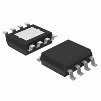
AOZ1034DI Alpha & Omega Semiconductor Inc, AOZ1034DI Datasheet - Page 11

AOZ1034DI
Manufacturer Part Number
AOZ1034DI
Description
IC BUCK SYNC ADJ 4A 8DFN
Manufacturer
Alpha & Omega Semiconductor Inc
Series
EZBuck™r
Type
Step-Down (Buck), PWM - Current Moder
Datasheet
1.AOZ1034DI.pdf
(18 pages)
Specifications of AOZ1034DI
Featured Product
The AOZ103x Family Synchronous Buck Regulator
Internal Switch(s)
Yes
Synchronous Rectifier
Yes
Number Of Outputs
1
Voltage - Output
0.8 V ~ 18 V
Current - Output
4A
Frequency - Switching
500kHz
Voltage - Input
4.5 V ~ 18 V
Operating Temperature
-40°C ~ 85°C
Mounting Type
Surface Mount
Package / Case
8-VDFN Exposed Pad
Lead Free Status / Rohs Status
Lead free / RoHS Compliant
Other names
785-1254-2
Available stocks
Company
Part Number
Manufacturer
Quantity
Price
To design the compensation circuit, a target crossover
frequency f
crossover frequency is where control loop has unity gain.
The crossover is the also called the converter bandwidth.
Generally a higher bandwidth means faster response to
load transient. However, the bandwidth should not be too
high because of system stability concern. When
designing the compensation loop, converter stability
under all line and load condition must be considered.
Usually, it is recommended to set the bandwidth to be
equal or less than 1/10 of switching frequency. The
AOZ1034 operates at a frequency range from 400kHz to
600kHz. It is recommended to choose a crossover
frequency equal or less than 40kHz.
The strategy for choosing R
cross over frequency with Rc and set the compensator
zero with C
to calculate R
where;
f
f
V
G
200 x 10
G
6.68 A/V.
The compensation capacitor C
make a zero. This zero is put somewhere close to the
dominate pole f
crossover frequency. C
The equation above can also be simplified to:
f
C
C
C
C
R
C
FB
EA
CS
Rev. 1.1 September 2010
is desired crossover frequency. For best performance,
is set to be about 1/10 of switching frequency,
C
C
C
=
is 0.8V,
is the error amplifier transconductance, which is
is the current sense circuit transconductance, which is
=
=
=
40kHz
-6
-----------------------------------
2π R
C
---------------------
f
C
A/V, and
O
R
×
C
C
×
×
. Using selected crossover frequency, f
C
for close loop must be selected. The system
--------- -
V
V
1.5
C
R
FB
:
O
p1
C
L
×
but lower than 1/5 of selected
×
f
P1
----------------------------- -
G
2π
EA
C
can is selected by:
×
×
C
C
G
C
and C
CS
c
and resistor R
C
is to set the
c
together
www.aosmd.com
C
,
An easy-to-use application software which helps to
design and simulate the compensation loop can be found
at www.aosmd.com.
Thermal Management and Layout
Consideration
In the AOZ1034 buck regulator circuit, high pulsing
current flows through two circuit loops. The first loop
starts from the input capacitors, to the VIN pin, to the
LX pins, to the filter inductor, to the output capacitor
and load, and then return to the input capacitor through
ground. Current flows in the first loop when the high side
switch is on. The second loop starts from inductor, to the
output capacitors and load, to the anode of the Schottky
diode, to the cathode of the Schottky diode. Current flows
in the second loop when the low side diode is on.
In PCB layout, minimizing the two loops area reduces the
noise of this circuit and improves efficiency. A ground
plane is strongly recommended to connect input
capacitor, output capacitor, and PGND pin of the
AOZ1034.
In the AOZ1034 buck regulator circuit, the major power
dissipating components are the AOZ1034 and the output
inductor. The total power dissipation of converter circuit
can be measured by input power minus output power.
The power dissipation of inductor can be approximately
calculated by output current and DCR of inductor.
The actual junction temperature can be calculated with
power dissipation in the AOZ1034 and thermal
impedance from junction to ambient.
The maximum junction temperature of AOZ1034 is
150ºC, which limits the maximum load current capability.
Please see the thermal de-rating curves for maximum
load current of the AOZ1034 under different ambient
temperature.
The thermal performance of the AOZ1034 is strongly
affected by the PCB layout. Extra care should be taken
by users during design process to ensure that the IC will
operate under the recommended environmental
conditions.
P
T
P
junction
inductor_loss
total_loss
=
=
(
P
V
=
total_loss
IN
I
O
×
2
I
×
IN
R
–
–
inductor
P
V
inductor_loss
O
×
I
O
×
1.1
) Θ
AOZ1034
×
Page 11 of 18
JA


