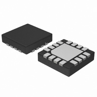
NCN4557MTR2G ON Semiconductor, NCN4557MTR2G Datasheet - Page 10

NCN4557MTR2G
Manufacturer Part Number
NCN4557MTR2G
Description
IC SMART CARD/SIM DUAL 16-QFN
Manufacturer
ON Semiconductor
Datasheet
1.NCN4557MTR2G.pdf
(12 pages)
Specifications of NCN4557MTR2G
Applications
*
Interface
*
Voltage - Supply
*
Package / Case
16-TFQFN Exposed Pad
Mounting Type
Surface Mount
Lead Free Status / RoHS Status
Lead free / RoHS Compliant
Available stocks
Company
Part Number
Manufacturer
Quantity
Price
Company:
Part Number:
NCN4557MTR2G
Manufacturer:
ON Semiconductor
Quantity:
405
the accelerator operates. During the first 200 ns (typical),
the slope of the rise time is solely a function of the pullup
resistor associated with the stray capacitance. During this
period, the PMOS devices are not activated since the input
voltage is below their V
crosses the V
providing a low impedance to charge the capacitance, thus
increasing the rise time as depicted in Figure 11. The same
mechanism applies for the opposite side of the line to make
sure the system is optimum.
Powerup Sequence
signals are LOW during the CRD_V
slope. The Powerup sequence is activated by setting the
ENABLE Boolean signal HIGH. CRD_RST, CRD_CLK
and CRD_I/O are maintained LOW during the activation
stage until CRD_V
The typical waveform provided in Figure 11 shows how
The powerup sequence makes sure all the card−related
Figure 11. CRD_IO Typical Rise and Fall Times
(33 pF capacitor connected on the board)
with Stray Capacitance > 30 pF
gsth
, the opposite one shot is activated,
CC
V
I/O
DD
reaches its nominal value (1.8 V or
gs
threshold. When the input slope
18 k
IO/CONTROL
CC
positive going
Figure 10. Basic I/O line Interface
Q1
200 ns
http://onsemi.com
NCN4557
LOGIC
10
GND
3.0 V). Figure 7 shows the typical NCN4557 activation
sequence.
voltage value, CRD_IO and CRD_RST are released.
second clock cycle after CRD_IO and CRD_RST are
enabled.
smart card signal sequence (contact activation sequence,
cold reset and warm reset sequences).
Powerdown Sequence
activated by setting the ENABLE Boolean signal LOW.
The communication I/O session is terminated immediately
according to the ISO7816 and EMV specifications as
depicted in Figures 8 and 13.
ISO7816 Sequence:
•
•
CRD_RSTA/B
CRD_CLKA/B
CRD_V
About 800 ms after CRD_V
CRD_CLK is enabled during the rising slope of the
In all cases the application software is responsible for the
The NCN4557 provides a powerdown sequence which is
CRD_IOA/B
CRD_RST is forced to LOW
CRD_CLK is forced to LOW 2 clock cycles after
ENABLE is set LOW unless CRD_CLK is already in
200 ns
ENABLE
CC
A/B
Q2
Figure 12. NCN4557 Power−Up
GND
T
Q3
ON
~ 0.9 ms
14 k
CC
CRD_V
has reached its nominal
CRD_I/O
2nd Rise Edge After
CRD_IOA/B Rising
CC


