MAX4886ETO+T Maxim Integrated Products, MAX4886ETO+T Datasheet - Page 6
MAX4886ETO+T
Manufacturer Part Number
MAX4886ETO+T
Description
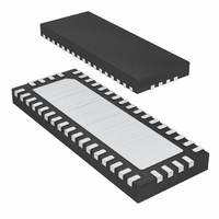
IC QUAD HDMI/DVI 2:1 SW 42-TQFN
Manufacturer
Maxim Integrated Products
Datasheet
1.MAX4886ETO.pdf
(12 pages)
Specifications of MAX4886ETO+T
Applications
Monitors, TV
Interface
DVI
Voltage - Supply
3 V ~ 3.6 V
Package / Case
42-TQFN Exposed Pad
Mounting Type
Surface Mount
Lead Free Status / RoHS Status
Lead free / RoHS Compliant
Other names
MAX4886ETO+T
MAX4886ETO+TTR
MAX4886ETO+TTR


The MAX4886 high-speed analog switch is ideal for
HDMI/DVI switching applications, permitting 2:1 or 1:2
switching. The MAX4886 contains four differential pairs
for HDMI or DVI switching. The MAX4886 connects either
one monitor to one of two digital video signals or one
HDMI/DVI output to one of two connectors or loads.
The MAX4886 differential switches are based on an
nFET architecture with an internal charge pump for gate
overdrive. This advanced architecture results in an
extremely low capacitance and on-resistance needed
for an excellent returns loss.
The MAX4886 features an 8Ω (typ) on-resistance and
2.5pF on-capacitance switches for routing RGB and
CLK video signals.
Quad, High-Speed HDMI/DVI 2:1 Digital
Video Switch
6
_______________________________________________________________________________________
COM3+
COM3-
COM1+
COM2+
COM2-
COM4+
COM4-
COM1-
SEL
GND
Detailed Description
MAX4886
Functional Diagram
V
DD
NO3+
NC4+
NC2+
NC3+
NO3-
NO4+
NC1+
NC1+
NO1+
NO1-
NC2-
NO2+
NC3-
NC4-
NO4-
NO2-
The MAX4886 switches are identical, and any of the
switches can be used to route RGB and CLK video
signals.
The device will also be useful in other high-speed
switching applications such as LVDS and LVPECL.
Signal inputs over the full voltage range (0V to V
passed through the switch with minimal change in on-
resistance (see the Typical Operating Characteristics
section). The switches are bidirectional. Therefore,
COM_, NC_, and NO_ can be either inputs or outputs.
The MAX4886 has a logic input that controls the switch
on/off function. Use SEL to switch COM_ to NO_ or
COM_ to NC_. Table 1 and the Functional Diagram
illustrate the MAX4886 Truth Table.
Proper power-supply sequencing is recommended for
all CMOS devices. Do not exceed the absolute
maximum ratings, because stresses beyond the listed
ratings can cause permanent damage to the device.
Always sequence V
inputs and the logic inputs. Bypass at least one V
input to ground with a 0.1µF capacitor as close to the
device as possible. Use the smallest physical size pos-
sible for optimal performance.
It is also recommended to bypass more than one V
input. A good strategy is to bypass one V
a 0.1µF capacitor and at least a second V
a 1nF to 10nF capacitor. (Use 0603 or smaller physical
size ceramic capacitor).
High-speed switches such as the MAX4886 require
proper PCB layout for optimum performance. Ensure
that impedance-controlled PCB traces for high-speed
signals are matched in length, and as short as possi-
ble. Connect the MAX4886 exposed paddle to a solid
ground plane.
Table 1. Switch Truth Table
Power-Supply Bypassing and Sequencing
SEL
0
1
Applications Information
COM_ to NC_
COM_ to NO_
DD
on first, followed by the switch
PC Board (PCB) Layout
Analog-Signal Levels
Logic Inputs (SEL)
FUNCTION
DD
DD
input with
input with
DD
) are
DD
DD
Related parts for MAX4886ETO+T
Image
Part Number
Description
Manufacturer
Datasheet
Request
R

Part Number:
Description:
MAX7528KCWPMaxim Integrated Products [CMOS Dual 8-Bit Buffered Multiplying DACs]
Manufacturer:
Maxim Integrated Products
Datasheet:
Part Number:
Description:
Single +5V, fully integrated, 1.25Gbps laser diode driver.
Manufacturer:
Maxim Integrated Products
Datasheet:
Part Number:
Description:
Single +5V, fully integrated, 155Mbps laser diode driver.
Manufacturer:
Maxim Integrated Products
Datasheet:
Part Number:
Description:
VRD11/VRD10, K8 Rev F 2/3/4-Phase PWM Controllers with Integrated Dual MOSFET Drivers
Manufacturer:
Maxim Integrated Products
Datasheet:
Part Number:
Description:
Highly Integrated Level 2 SMBus Battery Chargers
Manufacturer:
Maxim Integrated Products
Datasheet:
Part Number:
Description:
Current Monitor and Accumulator with Integrated Sense Resistor; ; Temperature Range: -40°C to +85°C
Manufacturer:
Maxim Integrated Products
Part Number:
Description:
TSSOP 14/A�/RS-485 Transceivers with Integrated 100O/120O Termination Resis
Manufacturer:
Maxim Integrated Products
Part Number:
Description:
TSSOP 14/A�/RS-485 Transceivers with Integrated 100O/120O Termination Resis
Manufacturer:
Maxim Integrated Products
Part Number:
Description:
QFN 16/A�/AC-DC and DC-DC Peak-Current-Mode Converters with Integrated Step
Manufacturer:
Maxim Integrated Products
Part Number:
Description:
TDFN/A/65V, 1A, 600KHZ, SYNCHRONOUS STEP-DOWN REGULATOR WITH INTEGRATED SWI
Manufacturer:
Maxim Integrated Products
Part Number:
Description:
Integrated Temperature Controller f
Manufacturer:
Maxim Integrated Products
Part Number:
Description:
SOT23-6/I�/45MHz to 650MHz, Integrated IF VCOs with Differential Output
Manufacturer:
Maxim Integrated Products
Part Number:
Description:
SOT23-6/I�/45MHz to 650MHz, Integrated IF VCOs with Differential Output
Manufacturer:
Maxim Integrated Products
Part Number:
Description:
EVALUATION KIT/2.4GHZ TO 2.5GHZ 802.11G/B RF TRANSCEIVER WITH INTEGRATED PA
Manufacturer:
Maxim Integrated Products
Part Number:
Description:
QFN/E/DUAL PCIE/SATA HIGH SPEED SWITCH WITH INTEGRATED BIAS RESISTOR
Manufacturer:
Maxim Integrated Products
Datasheet: