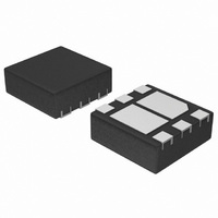
NIS1050MNTBG ON Semiconductor, NIS1050MNTBG Datasheet - Page 4

NIS1050MNTBG
Manufacturer Part Number
NIS1050MNTBG
Description
IC PMIC INTERFACE PROTECT 6-WDFN
Manufacturer
ON Semiconductor
Datasheet
1.NIS1050MNTBG.pdf
(5 pages)
Specifications of NIS1050MNTBG
Applications
Mobile Communications
Voltage - Supply
3 V ~ 30 V
Package / Case
6-VDFN Exposed Pad
Mounting Type
Surface Mount
Lead Free Status / RoHS Status
Lead free / RoHS Compliant
Interface
-
Lead Free Status / Rohs Status
Lead free / RoHS Compliant
Available stocks
Company
Part Number
Manufacturer
Quantity
Price
Company:
Part Number:
NIS1050MNTBG
Manufacturer:
ON
Quantity:
3 609
Company:
Part Number:
NIS1050MNTBG
Manufacturer:
ON Semiconductor
Quantity:
800
Part Number:
NIS1050MNTBG
Manufacturer:
ON/安森美
Quantity:
20 000
Mounting Considerations
to provide a low impedance path for the heat generated in
these devices. Both of these pads should have a solid
connection to as much board copper area as possible in order
to maintain a low operating temperature. The main purpose
of both of these pads is for thermal connections, not
electrical connections.
connected to the Vcc pin. This connection is optional and
will have a negligible difference in the electrical
performance of the chip due to the current into the LDO.
also have a low electrical impedance. Either pad 8, pad 6 or
both may be used for electrical connections. The total
The LDO and MOSFET are both attached to thermal pads
Pad 7 is the input voltage for the LDO. It is electrically
Pad 8 is the drain of the power MOSFET. This pad will
5
4
3
2
1
0
0
V
DS
Figure 4. On−Region Characteristics
, DRAIN−TO−SOURCE VOLTAGE (VOLTS)
1
V
GS
= 1.7 V to 8 V
2
5.30
5.25
5.20
5.15
5.10
5.05
5.00
4.95
4.90
4.85
4.80
−40
3
TYPICAL PERFORMANCE CURVES
−15
Figure 6. Output Voltage Variation with
T
J
, JUNCTION TEMPERATURE (°C)
4
T
J
10
= 25°C
http://onsemi.com
1.6 V
1.5 V
1.4 V
1.3 V
1.2 V
Temperature
35
5
4
impedance of the FET will not vary significantly since pad
6 is part of the lead-frame and therefore connected to pad 8
by a metal path on the lead frame. The majority of the
package impedance comes from the resistance between the
source and pin 1, since this is connected by bond wires.
Bypass Capacitors
without bypass capacitors; however, it is recommended to
use a low ESR capacitor if fast, ac transients or other
switching type currents will be present. Typically, a value of
1 to 10 nF is adequate for an output bypass capacitor. A 1 nF
capacitor may be added to the input if the input source is
noisy or if it has a high ac impedance due to long trace
lengths.
60
1.6
1.4
1.2
1.0
0.8
0.6
The LDO has been designed to operate in a stable mode
−50
I
V
D
GS
= 2 A
85
−25
= 4.5 V
Figure 5. On−Resistance Variation with
T
J
110
, JUNCTION TEMPERATURE (°C)
0
25
Temperature
50
75
100
125
150


