ISL54100ACQZ Intersil, ISL54100ACQZ Datasheet - Page 10
ISL54100ACQZ
Manufacturer Part Number
ISL54100ACQZ
Description
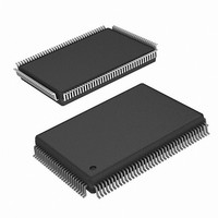
IC TMDS REGENERATOR MUX 128-MQFP
Manufacturer
Intersil
Datasheet
1.ISL54101ACQZ.pdf
(21 pages)
Specifications of ISL54100ACQZ
Applications
Multimedia Displays, Test Equipment
Interface
I²C
Voltage - Supply
3 V ~ 3.6 V
Package / Case
128-MQFP, 128-PQFP
Mounting Type
Surface Mount
Lead Free Status / RoHS Status
Lead free / RoHS Compliant
Available stocks
Company
Part Number
Manufacturer
Quantity
Price
Company:

Part Number:
ISL54100ACQZ
Manufacturer:
M/A-COM
Quantity:
43


Register Listing
0x03
ADDRESS
Input Control (0x12)
Recommended default: 0x62
REGISTER (DEFAULT VALUE)
(Continued)
10
ISL54100A, ISL54101A, ISL54102A
BIT(S)
0
1
2
3
4
5
6
7
Tri-state Unselected
Clock Inputs
Tri-state Unselected
Data Inputs
Tri-state Selected
Clock Inputs
Tri-state Selected
Data Inputs
Activity Detect Mode 0: AC Activity. Activity detection is based on the presence of
Clock Rx Hysteresis
Clock Rx Hysteresis
Magnitude
Recalibrate
FUNCTION NAME
0: Normal Operation
1: Termination of unselected TMDS clock inputs is tri-stated
to save power. Setting this bit will disable the activity detect
function. This bit should not be set in crosspoint
configuration because it will make the clock termination
resistance variable depending on which 2 inputs are
selected. In general, this bit should always be set to 0.
0: Normal Operation
1: Unselected Data inputs are tri-stated to save power. This
bit should not be set in crosspoint configuration because it
will make the data input termination resistance variable
depending on which 2 inputs are selected. (default)
0: Selected Clock inputs are terminated into
50Ω/100Ω.
1: Selected Clock inputs are tri-stated (to allow chip to
operate in parallel with another TMDS receiver with fixed
50Ω termination)
0: Selected Data inputs are terminated into
50Ω/100Ω.
1: Selected Data inputs are tri-stated (to allow chip to
operate in parallel with another TMDS receiver with fixed
50Ω termination)
AC activity on TMDS clock inputs. This setting (along with a
hysteresis of 20mV enabled) provides reliable activity
detection. (recommended setting)
1: Common Mode Voltage. If the common mode voltage is
above ~3.05V, the input is considered inactive. This method
has been found to be unreliable with small signal swings and
should not be used. This setting is the silicon default but
should be changed in software for more reliable activity
detection.
Enables hysteresis for the clock inputs to prevent false clock
detection when both inputs are high. Data inputs do not get
hysteresis.
0: TMDS input hysteresis disabled
1: TMDS input hysteresis enabled. Eliminates false activity
detects on unconnected channels. (recommended setting)
Controls the amount of hysteresis in the clock inputs.
0: 10mV
1: 20mV (recommended setting)
0: Normal Operation
1: Recalibrates termination resistance. To recalibrate, take
this bit high, wait at least 1ms, then take this bit low.
Calibration is automatically done after power-on, but
performing a recalibration after the supply voltage and
temperature have stabilized may result in termination
resistances closer to the desired 50Ω.
DESCRIPTION
June 17, 2008
FN6725.0
Related parts for ISL54100ACQZ
Image
Part Number
Description
Manufacturer
Datasheet
Request
R

Part Number:
Description:
TMDS Regenerators with Multiplexers
Manufacturer:
INTERSIL [Intersil Corporation]
Datasheet:

Part Number:
Description:
Intersil Corporation [CMOS Serial Controller Interface]
Manufacturer:
Intersil Corporation
Datasheet:
Part Number:
Description:
Manufacturer:
Intersil Corporation
Datasheet:
Part Number:
Description:
357-036-542-201 CARDEDGE 36POS DL .156 BLK LOPRO
Manufacturer:
Intersil Corporation
Datasheet:
Part Number:
Description:
1024-Word x 4-Bit LSI Static RAM
Manufacturer:
Intersil Corporation
Datasheet:
Part Number:
Description:
General Purpose NPN Transistor Arrays FN341.4
Manufacturer:
Intersil Corporation
Datasheet:
Part Number:
Description:
CMOS 16-Bit Microprocessor
Manufacturer:
Intersil Corporation
Datasheet:
Part Number:
Description:
Manufacturer:
Intersil Corporation
Datasheet:
Part Number:
Description:
Manufacturer:
Intersil Corporation
Datasheet:
Part Number:
Description:
Manufacturer:
Intersil Corporation
Datasheet:
Part Number:
Description:
Manufacturer:
Intersil Corporation
Datasheet:
Part Number:
Description:
CMOS 6-Bit Latch and Decoder Memory Interfaces
Manufacturer:
Intersil Corporation
Datasheet:
Part Number:
Description:
CA3046General Purpose NPN Transistor Arrays
Manufacturer:
Intersil Corporation
Datasheet:
Part Number:
Description:
Manufacturer:
Intersil Corporation
Datasheet: