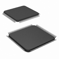
DS90CF388AVJDX/NOPB National Semiconductor, DS90CF388AVJDX/NOPB Datasheet - Page 15

DS90CF388AVJDX/NOPB
Manufacturer Part Number
DS90CF388AVJDX/NOPB
Description
IC DUAL PIX LDI 3.3V 100-TQFP
Manufacturer
National Semiconductor
Datasheet
1.DS90CF388AVJDXNOPB.pdf
(19 pages)
Specifications of DS90CF388AVJDX/NOPB
Applications
Displays
Interface
LVDS
Voltage - Supply
3 V ~ 3.6 V
Package / Case
100-TQFP, 100-VQFP
Mounting Type
Surface Mount
Lead Free Status / RoHS Status
Lead free / RoHS Compliant
Other names
DS90CF388AVJDX
Available stocks
Company
Part Number
Manufacturer
Quantity
Price
Company:
Part Number:
DS90CF388AVJDX/NOPB
Manufacturer:
Texas Instruments
Quantity:
10 000
Applications Information
HOW TO CONFIGURE THE DS90C387A AND
DS90CF388A FOR MOST COMMON APPLICATION
1. To configure for single input pixel-to-dual pixel output
application, the DS90C387 “DUAL” pin must be set to 1/2
Vcc=1.65V. This may be implemented using pull-up and
pull-down resistors of 10kΩ. In this configuration, the input
signals (single pixel) are split into odd and even pixel (dual
pixels) starting with the odd (first) pixel outputs A0-to-A3 the
next even (second) pixel outputs to A4-to-A7. The splitting of
the data signal also starts with DE (data enable) transitioning
from logic low to high indicating active data. The "R_FDE"
pin must be set high in this case. The number of clock cycles
during blanking must be an EVEN number. This configura-
tion will allow the user to interface to an LDI receiver
(DS90CF388A) or to two FPD-Link ’notebook’ receivers
(DS90CF384A or DS90CF386).
2. To configure for single pixel or dual pixel application using
the DS90C387A/DS90CF388A, the “DUAL” pin must be set
to Vcc (dual) or Gnd (single). In dual mode, the transmitter-
DS90C387A has two LVDS clock outputs enabling an inter-
face to two FPD-Link ’notebook’ receivers (DS90CF384A or
DS90CF386). In single mode, outputs A4-to-A7 and CLK2
are disabled which reduces power dissipation.
The DS90CF388A is able to support single or dual pixel
interface up to 112MHz operating frequency. This receiver
may also be used to interface to a VGA controller with an
integrated LVDS transmitter.
Note 12: This is based on testing with standard shield twisted pair cable. The amount of pre-emphasis will vary depending on the type of cable, length and operating
frequency.
RSKM - RECEIVER SKEW MARGIN
RSKM is a chipset parameter and is explained in AN-1059 in
detail. It is the difference between the transmitter’s pulse
position and the receiver’s strobe window. RSKM must be
greater than the summation of: Interconnect skew, LVDS
Source Clock Jitter (TJCC), and ISI (if any). See Figure 12.
Interconnect skew includes PCB traces differences, connec-
tor skew and cable skew for a cable application. PCB trace
and connector skew can be compensated for in the design of
the system. Cable skew is media type and length dependant.
1MΩ or NC
Frequency
112MHz
112MHz
80MHz
80MHz
65MHz
56MHz
100Ω
50kΩ
Rpre
9kΩ
3kΩ
1kΩ
TABLE 1. Pre-Emphasis DC Voltage Level With (Rpre)
TABLE 2. Pre-Emphasis Needed Per Cable Length
Resulting PRE Voltage
PRE Voltage
0.75V
1.0V
1.5V
2.0V
2.6V
1.0V
1.5V
1.0V
1.2V
1.5V
1.0V
Vcc
15
TRANSMITTER FEATURES
The transmitter is designed to reject cycle-to-cycle jitter
which may be seen at the transmitter input clock. Very low
cycle-to-cycle jitter is passed on to the transmitter outputs.
This significantly reduces the impact of jitter provided by the
input clock source, and improves the accuracy of data sam-
pling.
The transmitter is offered with programmable edge data
strobes for convenient interface with a variety of graphics
controllers. The transmitter can be programmed for rising
edge strobe or falling edge strobe through a dedicated pin. A
rising edge transmitter will inter-operate with a falling edge
receiver without any translation logic.
PRE-EMPHASIS
Pre-Emphasis adds extra current during LVDS logic transi-
tion to reduce the cable loading effects. Pre-emphasis
strength is set via a DC voltage level applied from min to max
(0.75V to Vcc) at the “PRE” pin. A higher input voltage on the
”PRE” pin increases the magnitude of dynamic current dur-
ing data transition. The “PRE” pin requires one pull-up resis-
tor (Rpre) to Vcc in order to set the DC level. There is an
internal resistor network, which cause a voltage drop. Please
refer to the tables below to set the voltage level.
POWER DOWN
Both transmitter and receiver provide a power down feature.
When asserted current draw through the supply pins is
minimized and the PLLs are shut down. The transmitter
outputs are in TRI-STATE when in power down mode. The
receiver outputs are forced to a active LOW state when in
the power down mode. (See Pin Description Tables). The PD
pin should be driven HIGH to enable the device once V
stable.
Typical cable length
100% pre-emphasis
50% pre-emphasis
Standard LVDS
10 meters
10 meters
2 meters
5 meters
2 meters
7 meters
Effects
www.national.com
CC
is


