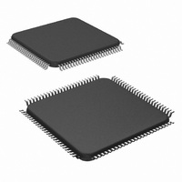
DS90C387RVJDX/NOPB National Semiconductor, DS90C387RVJDX/NOPB Datasheet - Page 3

DS90C387RVJDX/NOPB
Manufacturer Part Number
DS90C387RVJDX/NOPB
Description
IC LDI DUAL PIXAL 3.3V 100-TQFP
Manufacturer
National Semiconductor
Datasheet
1.DS90C387RVJDXNOPB.pdf
(28 pages)
Specifications of DS90C387RVJDX/NOPB
Applications
Displays
Interface
2-Wire Serial
Voltage - Supply
3 V ~ 3.6 V
Package / Case
100-TQFP, 100-VQFP
Mounting Type
Surface Mount
Lead Free Status / RoHS Status
Lead free / RoHS Compliant
Other names
DS90C387RVJDX
Available stocks
Company
Part Number
Manufacturer
Quantity
Price
Company:
Part Number:
DS90C387RVJDX/NOPB
Manufacturer:
Texas Instruments
Quantity:
10 000
LVCMOS/LVTTL DC SPECIFICATIONS ( All pins, except output pins AnP, AnM, CLKnP and CLKnM, BAL, PD pins)
V
V
V
I
V
LVCMOS DC SPECIFICATIONS ( PD pin)
V
V
V
I
LVDS DRIVER DC SPECIFICATIONS (output pins AnP, AnM, CLKnP and CLKnM)
V
∆V
V
∆V
I
I
Low Voltage Mode DC SPECIFICATIONS( pins D0 to D23, CLKINP, CLKINM, DE, HSYNC,VSYNC)
V
V
V
IN
IN
OS
OZ
Symbol
IH
IL
CL
OL
IH
IL
CL
OD
OS
IHLS
ILLS
REF
Absolute Maximum Ratings
If Military/Aerospace specified devices are required,
please contact the National Semiconductor Sales Office/
Distributors for availability and specifications.
Electrical Characteristics
Over recommended operating supply and temperature ranges unless otherwise specified.(Note 2)
OD
OS
Supply Voltage (V
LVCMOS/LVTTL Output
Voltage
LVDS Driver Output
Voltage
LVDS Output Short
Circuit
Junction Temperature
Storage Temperature
Lead Temperature
Maximum Package Power Dissipation Capacity
25˚C
(Soldering, 4 sec.)
High Level Input Voltage
Low Level Input Voltage
Input Clamp Voltage
Input Current
Low level Open Drain Output
Voltage
High Level Input Voltage
Low Level Input Voltage
Input Clamp Voltage
Input Current
Differential Output Voltage
Change in V
Complimentary Output States
Offset Voltage
Change in V
Complimentary Output States
Output Short Circuit Current
Output TRI-STATE
Low Swing High Level Input
Voltage, V
Low Swing Low Level Input
Voltage,V
Differential Input Reference
Voltage, V
Duration
CC
CC
CC
CC
Parameter
OD
OS
)
= 3V
= 3V
= 3V
between
between
®
Current
−0.3V to (V
−0.3V to (V
−65˚C to +150˚C
−0.3V to +4V
Continuous
V
V
I
V
V
I
V
V
I
V
V
R
V
PD = 0V, V
Low Swing,V
CC
CC
CL
OL
CL
(Note 1)
REF
REF
IN
IN
REF
REF
IN
IN
L
OUT
= 100Ω
+ 0.3V)
+ 0.3V)
+150˚C
+260˚C
= 18 mA
= 18 mA
= 2 mA
= 0.4V, or V
= GND
= 0.4V, or V
= GND
@
= V
= V
= V
= V
= 0V, R
CC3V
CC3V
CC3V
CC3V
OUT
REF
L
Conditions
= V
= V
= V
= V
= 100Ω
= 0V or V
CC
CC
=
3
CC
CC
CC
CC
1
⁄
2
Recommended Operating
Conditions
V
All Supply Voltage
Operating Free Air
Supply Noise Voltage (V
to 33MHz
DDQ
Package Derating:
ESD Rating:
Temperature (T
CC
100 TQFP Package:
DS90C387R
(HBM, 1.5kΩ, 100pF)
(EIAJ, 0Ω, 200pF)
A)
GND
+100mV
1.125
GND
GND
V
0.45
Min
−15
−15
247
2.0
2.9
REF
CC
)up
18.2mW/˚C above +25˚C
Min Nom Max
−10
3.0
0.5*V
+1.8
+1.8
1.25
−3.5
Typ
-0.8
-0.8
345
0.1
±
0
0
1
DDQ
+25
3.3
+70
3.6
-100mV
1.475
V
100 mV
www.national.com
>
Max
V
-1.5
+15
V
-1.5
+15
−11
±
550
0.8
0.3
0.8
1.8
35
35
REF
>
CC
CC
1
10
300 V
2.8W
2 kV
Units
˚C
V
p-p
Units
mV
mV
mV
mA
µA
µA
µA
µA
µA
V
V
V
V
V
V
V
V
V
V
V


