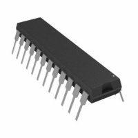
AD7868AN Analog Devices Inc, AD7868AN Datasheet - Page 3

AD7868AN
Manufacturer Part Number
AD7868AN
Description
IC I/O PORT 12BIT ANLG 24-DIP
Manufacturer
Analog Devices Inc
Datasheet
1.AD7868ARZ-REEL.pdf
(16 pages)
Specifications of AD7868AN
Rohs Status
RoHS non-compliant
Applications
Analog I/O
Interface
TTL/CMOS
Voltage - Supply
4.75 V ~ 5.25 V
Package / Case
24-DIP (0.300", 7.62mm)
Mounting Type
Through Hole
Converter Type
ADC/DAC
Resolution
12b
Number Of Dac's
Single
Data Rate
0.083MSPS
Digital Interface Type
Serial (2-Wire)
Pin Count
24
Package Type
PDIP
Lead Free Status / Rohs Status
Not Compliant
Available stocks
Company
Part Number
Manufacturer
Quantity
Price
Company:
Part Number:
AD7868AN
Manufacturer:
SONY
Quantity:
6 252
DAC SECTION
REV. B
Parameter
DYNAMIC PERFORMANCE
DC ACCURACY
REFERENCE OUTPUT
REFERENCE INPUT
LOGIC INPUTS (LDAC, TFS, TCLK, DT)
ANALOG INPUT
AC CHARACTERISTICS
POWER REQUIREMENTS
NOTES
1
2
3
4
5
6
7
Specifications subject to change without notice.
Temperature ranges are as follows: A/B Versions, –40 C to +85 C; T Version, –55 C to +125 C.
V
SNR calculation includes distortion and noise components.
Using external sample and hold.
Measured with respect to RI DAC and includes bipolar offset error.
For capacitive loads greater than 50 pF a series resistor is required
Sample tested @ +25 C to ensure compliance.
(see INTERNAL REFERENCE section).
OUT
Signal-to-Noise Ratio
Total Harmonic Distortion (THD)
Peak Harmonic or Spurious Noise
Resolution
Integral Nonlinearity
Integral Nonlinearity
Differential Nonlinearity
Bipolar Zero Error
Positive Full-Scale Error
Negative Full-Scale Error
RO ADC @ +25 C
RO ADC TC
RO ADC TC
Reference Load Change ( RO DAC vs. I)
RI DAC Input Range
Input Current
Input High Voltage, V
Input Low Voltage, V
Input Current, I
Input Capacitance, C
Output Voltage Range
dc Output Impedance
Short-Circuit Current
Voltage Output Settling-Time
Digital-to-Analog Glitch Impulse
Digital Feedthrough
V
IN
T
Positive Full-Scale Change
Negative Full-Scale Change
MIN
(pk–pk) = 3 V.
to V
to T
OUT
MAX
Isolation
IN
IN
3
INL
INH
(V
Load to AGND; R
(SNR) @ +25 C
6
7
5
7
DD
5
= +5 V
2
5%, V
L
= 2 k , C
SS
= –5 V
A
Version
70
70
–78
–78
12
2.99/3.01 2.99/3.01 2.99/3.01
–1.5
2.85/3.15 2.85/3.15 2.85/3.15
1
2.4
0.8
10
0.3
20
3
3
10
2
100
As per ADC Section
1/2
0.9
5
5
5
25
10
3
L
= 100 pF. All specifications T
1
5%, AGND = DGND = 0 V, RI DAC = +3 V and decoupled as shown in Figure 2, V
B
Version
72
71
–78
–78
12
–1.5
1
2.4
0.8
10
0.3
20
3
3
10
2
100
1/2
1
0.9
5
5
5
25
40
10
3
1
T
Version
70
70
–76
–76
12
–1.5
1
2.4
0.8
10
0.3
20
3
3
10
2
100
–3–
1/2
1
0.9
5
5
5
25
50
10
3
Model
AD7868AN
AD7868AQ
AD7868BN
AD7868BQ
AD7868AR
AD7868BR
*N = Plastic DIP; Q = Cerdip; R = SOIC (Small Outline IC).
1
Units
dB min
dB min
dB max
dB max
Bits
LSB typ
LSB max
LSB max
LSB max
LSB max
LSB max
V min/V max
ppm/ C typ
ppm/ C max
mV max
V min/V max 3 V
V min
V max
pF max
V nom
mA typ
nV secs typ
nV secs typ
dB typ
MIN
A max
A max
s max
s max
typ
to T
MAX
Temperature
Range
–40 C to +85 C
–40 C to +85 C
–40 C to +85 C
–40 C to +85 C
–40 C to +85 C
–40 C to +85 C
unless otherwise noted.)
Typically 71.5 dB at +25 C for 0 < V
V
V
Reference Load Current Change (0–500 A)
DAC Code Change All 1s to All 0s
Test Conditions/Comments
V
Typically –84 dB at +25 C for 0 < V
Typically –84 dB at +25 C for 0 < V
Guaranteed Monotonic
V
V
V
Settling Time to Within 1/2 LSB of Final Value
Typically 2 s
Typically 2.5 s
V
ORDERING GUIDE
OUT
OUT
OUT
DD
DD
IN
IN
= 0 V to V
= 3 V, 41.5 kHz Sine Wave
= 5 V
= 5 V
= 1 kHz Sine Wave, f
= 1 kHz Sine Wave, f
= 1 kHz Sine Wave, f
5%
5%
5%
DD
SNR
70 dB
70 dB
72 dB
72 dB
70 dB
72 dB
Relative
Accuracy
(LSB)
SAMPLE
SAMPLE
SAMPLE
1/2 typ
1/2 typ
1 max
1 max
1/2 typ
1 max
= 83 kHz
= 83 kHz
= 83 kHz
OUT
OUT
OUT
AD7868
< 20 kHz
< 20 kHz
Package
Q-24
N-24
Q-24
R-28
Option*
N-24
R-28
< 20 kHz
OUT
4
4
4


