DS33X11+ Maxim Integrated Products, DS33X11+ Datasheet - Page 86

DS33X11+
Manufacturer Part Number
DS33X11+
Description
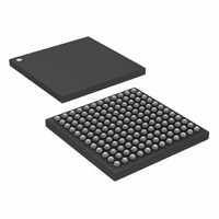
IC MAPPING ETHERNET 144CSBGA
Manufacturer
Maxim Integrated Products
Datasheet
1.DS33X11.pdf
(375 pages)
Specifications of DS33X11+
Applications
Data Transport
Interface
SPI
Voltage - Supply
1.8V, 2.5V, 3.3V
Package / Case
144-CSBGA
Mounting Type
Surface Mount
Lead Free Status / RoHS Status
Lead free / RoHS Compliant
- Current page: 86 of 375
- Download datasheet (3Mb)
8.20 Ethernet Frame Encapsulation
The figure below depicts the Layer 1 mapping and Layer 2 protocol encapsulation options available:
8.20.1 Transmit Packet Processor (Encapsulator)
The data from each WAN Group is processed by the Transmit Packet Processor (or Encapsulator) before being
transmitted on the Serial interfaces. The Encapsulator performs bit reordering, FCS processing, frame error
insertion, stuffing, frame abort sequence insertion, inter-frame padding, VLAN tag insertion, MPLS tag insertion,
PPP Headers, LAPS Headers, octet removal, and frame scrambling. Each WAN Group’s encapsulation settings
can be independently configured with the PP.EMCR(1-4) registers.
The Encapsulator automatically inserts the inter-frame fill and flag characters based on the selection of
HDLC/cHDLC/LAPS or GFP in PP.EMCR.EPRTSEL. A Line Header Insertion function (in PP.ELHHR and
PP.ELHLR) allows the user to insert Address, Control, and Protocol bytes for HDLC/cHDLC/X.86, or Type and
tHEC bytes for GFP. The Tag 1 Insertion function (in PP.ET1DHR and PP.ET1DLR) allows the user to insert a 4-
byte MPLS tag immediately before the Destination Address (DA). The Tag 2 Insertion function (in PP.ET2DHR and
PP.ET2DLR) allows the user to insert a 4-byte VLAN tag immediately after the Source Address (SA). Any existing
VLAN tags are “pushed” lower in the frame.
HDLC processing can be disabled. Disabling HDLC processing disables FCS processing, frame error insertion,
stuffing, frame abort sequence insertion, and inter-frame fill/padding. Only bit reordering and frame scrambling are
not disabled.
Bit reordering changes the bit order of each byte. If bit reordering is disabled, the outgoing 8-bit data stream
DT[1:8] with DT[1] being the MSB and DT[8] being the LSB is output from the Transmit FIFO with the MSB in
TFD[7] (or 15, 23, or 31) and the LSB in TFD[0] (or 8, 16, or 24) of the transmit FIFO data TFD[7:0] 15:8, 23:16, or
31:24). If bit reordering is enabled, the outgoing 8-bit data stream DT[1:8] is output from the Transmit FIFO with the
MSB in TFD[0] and the LSB in TFD[7] of the transmit FIFO data TFD[7:0]. In bit synchronous mode, DT [1] is the
first bit transmitted. Bit reordering is configured using the PP.EMCR.TBRE bit. Note that bit reordering is not
available in the A1 device revision (GL.IDR.REVn=000).
FCS processing, when enabled in PP.EMCR(1-4), appends a calculated FCS to the frame. The polynomial used
for FCS-16 is x
x
not performed.
Frame error insertion inserts errors into the GFP PLI, data unit, or FCS bytes. A single bit is corrupted in each
errored frame. The location of the corrupted bit is user-programmable. Error insertion is controlled by the PP.EEIR
register.
Rev: 063008
7
________________________________________________ DS33X162/X161/X82/X81/X42/X41/X11/W41/W11
+ x
5
+ x
(PDH Interfaces)
4
+ x
16
2
WAN
+ x + 1. The FCS is inverted after calculation. If packet processing is disabled, FCS processing is
+ x
12
+ x
5
+ 1. The polynomial used for FCS-32 is x
GFP-F
MPLS / VLAN Tagging
Synchronous Links
LAPS cHDLC
VCAT
IEEE 802.1D Bridge
HDLC
32
+ x
26
+ x
Traffic
802.3
23
Mgmt
MAC
+ x
22
+ x
16
+ x
12
+ x
11
Side
LAN
+ x
86 of 375
10
+ x
8
+
Related parts for DS33X11+
Image
Part Number
Description
Manufacturer
Datasheet
Request
R

Part Number:
Description:
MAX7528KCWPMaxim Integrated Products [CMOS Dual 8-Bit Buffered Multiplying DACs]
Manufacturer:
Maxim Integrated Products
Datasheet:

Part Number:
Description:
Single +5V, fully integrated, 1.25Gbps laser diode driver.
Manufacturer:
Maxim Integrated Products
Datasheet:

Part Number:
Description:
Single +5V, fully integrated, 155Mbps laser diode driver.
Manufacturer:
Maxim Integrated Products
Datasheet:

Part Number:
Description:
VRD11/VRD10, K8 Rev F 2/3/4-Phase PWM Controllers with Integrated Dual MOSFET Drivers
Manufacturer:
Maxim Integrated Products
Datasheet:

Part Number:
Description:
Highly Integrated Level 2 SMBus Battery Chargers
Manufacturer:
Maxim Integrated Products
Datasheet:

Part Number:
Description:
Current Monitor and Accumulator with Integrated Sense Resistor; ; Temperature Range: -40°C to +85°C
Manufacturer:
Maxim Integrated Products

Part Number:
Description:
TSSOP 14/A�/RS-485 Transceivers with Integrated 100O/120O Termination Resis
Manufacturer:
Maxim Integrated Products

Part Number:
Description:
TSSOP 14/A�/RS-485 Transceivers with Integrated 100O/120O Termination Resis
Manufacturer:
Maxim Integrated Products

Part Number:
Description:
QFN 16/A�/AC-DC and DC-DC Peak-Current-Mode Converters with Integrated Step
Manufacturer:
Maxim Integrated Products

Part Number:
Description:
TDFN/A/65V, 1A, 600KHZ, SYNCHRONOUS STEP-DOWN REGULATOR WITH INTEGRATED SWI
Manufacturer:
Maxim Integrated Products

Part Number:
Description:
Integrated Temperature Controller f
Manufacturer:
Maxim Integrated Products

Part Number:
Description:
SOT23-6/I�/45MHz to 650MHz, Integrated IF VCOs with Differential Output
Manufacturer:
Maxim Integrated Products

Part Number:
Description:
SOT23-6/I�/45MHz to 650MHz, Integrated IF VCOs with Differential Output
Manufacturer:
Maxim Integrated Products

Part Number:
Description:
EVALUATION KIT/2.4GHZ TO 2.5GHZ 802.11G/B RF TRANSCEIVER WITH INTEGRATED PA
Manufacturer:
Maxim Integrated Products

Part Number:
Description:
QFN/E/DUAL PCIE/SATA HIGH SPEED SWITCH WITH INTEGRATED BIAS RESISTOR
Manufacturer:
Maxim Integrated Products
Datasheet:


