AD8159ASVZ Analog Devices Inc, AD8159ASVZ Datasheet - Page 3
AD8159ASVZ
Manufacturer Part Number
AD8159ASVZ
Description
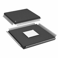
IC MUX/DEMUX QUAD BUFF 100TQFP
Manufacturer
Analog Devices Inc
Series
XStream™r
Datasheet
1.AD8159ASVZ.pdf
(24 pages)
Specifications of AD8159ASVZ
Applications
2:1 Multiplexer/1:2 De-Multiplexer
Interface
Serial
Voltage - Supply
3 V ~ 3.6 V
Package / Case
100-TQFP Exposed Pad, 100-eTQFP, 100-HTQFP, 100-VQFP
Mounting Type
Surface Mount
Crosspoint Switch Type
Digital
Input / Output Configuration
LVPECL, CML / CML
Control Interface
Parallel
Supply Voltage Range
3V To 3.6V
Operating Temperature Range
-40°C To +85°C
Lead Free Status / RoHS Status
Lead free / RoHS Compliant
Available stocks
Company
Part Number
Manufacturer
Quantity
Price
Company:

Part Number:
AD8159ASVZ
Manufacturer:
Analog Devices Inc
Quantity:
135
Company:
Part Number:
AD8159ASVZ
Manufacturer:
AnalogDevices
Quantity:
321
Company:
Part Number:
AD8159ASVZ
Manufacturer:
ADI
Quantity:
174
Company:
Part Number:
AD8159ASVZ
Manufacturer:
Analog Devices Inc
Quantity:
10 000
Part Number:
AD8159ASVZ
Manufacturer:
ADI/亚德诺
Quantity:
20 000


SPECIFICATIONS
V
800 mV p-p, T
Table 1.
Parameter
DYNAMIC PERFORMANCE
INPUT CHARACTERISTICS
OUTPUT CHARACTERISTICS
TERMINATION CHARACTERISTICS
POWER SUPPLY
THERMAL CHARACTERISTICS
LOGIC INPUT CHARACTERISTICS
1
2
3
BICAST off, loopback off on all ports, pre-emphasis off on all ports, equalization set to minimum on all ports.
V
V
CC
ICM
ID
Data Rate/Channel (NRZ)
Deterministic Jitter
Random Jitter
Propagation Delay
Lane-to-Lane Skew
Switching Time
Output Rise/Fall Time
Input Voltage Swing
Input Voltage Range
Input Bias Current
Input Capacitance
Output Voltage Swing
Output Voltage Range
Output Current
Output Capacitance
Resistance
Temperature Coefficient
Operating Range
Supply Current
Supply Current
Operating Temperature Range
θ
θ
θ
Input Voltage High, V
Input Voltage Low, V
is the input differential peak-to-peak voltage swing.
JA
JB
JC
= 3.3 V, V
is the input common-mode voltage.
V
V
I
I
I
I
I/O
I/O
CC
CC
CC
TTI
= I
= I
, V
TTO
TTO
TTO
+ I
+ I
, V
EE
A
TTOI
TTOI
TTIO
= 0 V, R
= 25°C, unless otherwise noted.
, V
+ I
+ I
TTOI
TTI
TTI
+ I
+ I
IL
IH
L
TTIO
TTIO
= 50 Ω, basic configuration,
Conditions
Data rate = 3.2 Gbps; see Figure 21
RMS; see Figure 24
Input to output
20% to 80%
Port C, differential, V
Port A/Port B, differential, V
Common mode, V
Differential, PE = 0
Single-ended absolute voltage level; see Figure 26
Port A/Port B, PE_A/PE_B = 0
Port C, PE_C = 0
Port A/Port B, PE_A/PE_B = 3
Port C, PE_C = 3
Differential
V
Basic configuration,
swings (800 mV p-p differential), 50 Ω far-end terminations
BICAST = 1, PE = 3 on all ports, dc-coupled inputs/outputs,
400 mV I/O swings (800 mV p-p differential), 50 Ω far-end
terminations
Still air
Still air
Still air
EE
= 0 V
1
ID
data rate = 3.2 Gbps, input common-mode voltage = 2.7 V, differential input swing =
3
1
ICM
= 800 mV p-p; see Figure 25
dc-coupled inputs/outputs, 400 mV I/O
2
= V
Rev. B | Page 3 of 24
ICM
CC
2
− 0.6 V; see Figure 22
= V
CC
− 0.6 V; see Figure 22
Min
DC
200
100
V
V
90
2.4
−40
2.4
V
3.0
EE
CC
EE
+ 1.8
− 1.6
Typ
20
1
600
100
5
100
4
2
800
16
20
28
32
2
100
0.15
3.3
3.3
175
144
255
352
29
16
13
Max
3.2
2000
2000
V
V
110
3.6
3.6
+85
V
0.8
CC
CC
CC
+ 0.3
+ 0.6
AD8159
Unit
Gbps
ps p-p
ps
ps
ps
ns
ps
mV p-p
mV p-p
V
μA
pF
mV p-p
V
mA
mA
mA
mA
pF
Ω
Ω/°C
V
V
mA
mA
mA
mA
°C
°C/W
°C/W
°C/W
V
V
Related parts for AD8159ASVZ
Image
Part Number
Description
Manufacturer
Datasheet
Request
R

Part Number:
Description:
SENSOR GAS FOR CO/NO2 EXHAUST
Manufacturer:
GE Sensing
Datasheet:

Part Number:
Description:
±1.7g Dual-Axis IMEMS Accelerometer Evaluation Board
Manufacturer:
Analog Devices Inc
Datasheet:

Part Number:
Description:
Inertial Sensor Evaluation System
Manufacturer:
Analog Devices Inc
Datasheet:
Part Number:
Description:
Manufacturer:
Analog Devices Inc
Datasheet:
Part Number:
Description:
Manufacturer:
Analog Devices Inc
Datasheet:
Part Number:
Description:
Manufacturer:
Analog Devices Inc
Datasheet:
Part Number:
Description:
Manufacturer:
Analog Devices Inc
Datasheet:
Part Number:
Description:
Manufacturer:
Analog Devices Inc
Datasheet:
Part Number:
Description:
Manufacturer:
Analog Devices Inc
Datasheet:
Part Number:
Description:
Manufacturer:
Analog Devices Inc
Datasheet:
Part Number:
Description:
Manufacturer:
Analog Devices Inc
Datasheet:
Part Number:
Description:
Manufacturer:
Analog Devices Inc
Datasheet:
Part Number:
Description:
Manufacturer:
Analog Devices Inc
Datasheet: