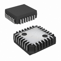
TP3465V/NOPB National Semiconductor, TP3465V/NOPB Datasheet - Page 4

TP3465V/NOPB
Manufacturer Part Number
TP3465V/NOPB
Description
IC INTERFACE MICRWIRE DEV 28PLCC
Manufacturer
National Semiconductor
Datasheet
1.TP3465VNOPB.pdf
(17 pages)
Specifications of TP3465V/NOPB
Applications
ISDN
Interface
Serial EEPROM
Voltage - Supply
4.5 V ~ 5.5 V
Package / Case
28-PLCC
Mounting Type
Surface Mount
Lead Free Status / RoHS Status
Lead free / RoHS Compliant
Other names
*TP3465V
*TP3465V/NOPB
TP3465V
*TP3465V/NOPB
TP3465V
Available stocks
Company
Part Number
Manufacturer
Quantity
Price
Company:
Part Number:
TP3465V/NOPB
Manufacturer:
ADI
Quantity:
63
Company:
Part Number:
TP3465V/NOPB
Manufacturer:
Texas Instruments
Quantity:
10 000
Non-Multiplexed Microprocessor Interface
The MULT INT pin is sampled on power-up and if not LOW the microprocessor bus format is assumed to be Non-multiplexed
This interface consists of a four-bit Address bus an eight-bit Data bus and six control lines (CE RST AS MI RD DS
WR (R WR) and the INT signal if enabled)
Functional Description
The block diagram of the MICROWIRE Interface Device
(MID) is shown in Figure 1 It essentially consists of a very
flexible microprocessor bus interface a serial MICROWIRE
interface and a Chip Select (output) port Internally it con-
tains a programmable clock divider to derive the MICRO-
WIRE clock speed from a system clock
MICROPROCESSOR INTERFACE
The Microprocessor bus interface supports both National
Intel and Motorola bus formats in the Multiplexed and Non-
multiplexed bus modes
The MULT INT pin is sampled on power-up and if LOW the
microprocessor bus format is assumed to be Multiplexed
and the pin is considered an input pin to indicate Multi-
plexed bus format The pin is internally pulled HIGH Upon
sampling if the pin is not LOW the bus format is assumed
to be Non-multiplexed
The microprocessor interface supports multiplexed Ad-
dress Data Formats for the Intel 8088 80188 and Motorola
6803 families to work in 8-bit mode Non-multiplexed busses
of the National 32000 Intel 80286 and Motorola 68000 se-
ries processors and similar are supported in the TP3465 28-
pin part Four address lines allow access to all MID regis-
ters
The MID incorporates a flexible bus interface logic to sup-
port the different address and data strobes required by the
different bus formats The timing specifications are shown in
a later section The following table shows microprocessor
bus control pin functions
See Figure 7 for connection of the AS and DS signals to
Motorola Ps
AS MI
RD DS
WR (R W)
MID Pin
RST
MULT
INT
Name
MUXed
ALE
WR
RD
NSC Intel Bus
Pin No
28 Pkg
Non-MUXed
22
18
MI
WR
RD
e
1
MUXed
(R W)
AS
DS
Motorola Bus
Type
O
I
I
Non-MUXed
MI
(R W)
DS
e
0
The RST is the master Reset input when LOW it forces the
device in the RESET condition (same as Power-on-Reset)
Multiplexed Bus input or INTerrupt output It is internally pulled
HIGH to indicate a Non-multiplexed bus format and the pin can
be an INT output pin if enabled by setting the Inten bit in the
CKR register INT pulls low to indicate the completion of a
MICROWIRE transfer operation
4
MICROWIRE COMMUNICATION MODES
The MID provides a MICROWIRE port to the main proces-
sor having two modes of operation with the MICROWIRE
peripherals software-controlled chip select and hard-
ware-generated chip select modes
In the first scheme besides the 2 data byte registers there
is a third register which maps directly with the output CS
Chip Selects pins, which there eight pins for this function in
the TP3465 28-pin package . The software in the microproc-
essor then writes to the CS register to select and deselect
individual bits (corresponding to pins)
In the second scheme the CS pins are activated by a hard-
ware state machine when triggered by accessing the data
registers through other address locations (see section on
Register description) In this case the hardware will activate
the chip select pin send the appropriate number of MICRO-
WIRE data bits (8 or 16 ) and then deselect the pin. This
enhanced mode of communication allows the MICROWIRE
peripheral devices to appear as if I O mapped in the micro-
processor’s memory space
CONTROL AND DATA REGISTERS
There are 6 control registers (PD MWM SKP SKR ST and
CS) and 1 set of Data registers (First MICROWIRE Byte
FMB and Second MICROWIRE Byte SMB) for data com-
munication to MICROWIRE devices In normal mode the
Chip select pins CS0 –C7 are controlled (via the CS register)
by software and data is transferred via the FMB and SMB
registers located at address 01h and 00h (see Table I)
Eight additional addresses (FMBD0 –7) access the same
data register (FMB) but provide additional information to
an internal state machine which drives appropriate chip se-
lect pins (e g FMBD0 at address 02h controls CS0 pin
FMBD1 at address 03h controls CS1 pin etc ) There is
only 1 set of Data registers (FMB and SMB) which han-
dle the MICROWIRE communication This latter method
of allocating special addresses to provide pin-select infor-
mation facilitates an enhanced MICROWIRE interface to
the host processor
Table I summarizes the Control and Data Registers and the
addresses at which they are accessed
(Continued)
Function


