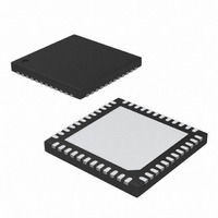
MAX9218ETM+ Maxim Integrated Products, MAX9218ETM+ Datasheet

MAX9218ETM+
Specifications of MAX9218ETM+
Related parts for MAX9218ETM+
MAX9218ETM+ Summary of contents
Page 1
... Separate Output Supply Allows Interface to 1.8V to 3.3V Logic ♦ +3.3V Core Power Supply ♦ Space-Saving Thin QFN and LQFP Packages ♦ -40°C to +85°C Operating Temperature Applications PART MAX9218ECM+ MAX9218ECM/V+ MAX9218ETM+ + Denotes a lead(Pb)-free/RoHS-compliant package. /V denotes an automotive qualified part Exposed pad. DE_OUT 24 23 CNTL_OUT8 V ...
Page 2
DC-Balanced LVDS Deserializer ABSOLUTE MAXIMUM RATINGS V to _GND........................................................-0.5V to +4.0V CC_ Any Ground to Any Ground...................................-0.5V to +0.5V IN+, IN- to LVDS GND...........................................-0.5V to +4.0V IN+, IN- Short Circuit to LVDS GND or V IN+, IN- Short ...
Page 3
DC ELECTRICAL CHARACTERISTICS (continued) = +3.0V to +3.6V, PWRDWN = high, differential input voltage ⏐V (V CC_ - ⏐ /2⏐ -40°C to +85°C, unless otherwise noted. Typical values are ...
Page 4
DC-Balanced LVDS Deserializer AC ELECTRICAL CHARACTERISTICS = 8pF, PWRDWN = high, differential input voltage ⏐ +3.0V to 3.6V, C CC_ L = ⏐V - ⏐V V /2⏐ /2⏐ -40°C to +85°C, unless ...
Page 5
C = 8pF +25°C, unless otherwise noted WORST-CASE PATTERN SUPPLY CURRENT vs. FREQUENCY FREQUENCY (MHz) OUTPUT TRANSITION TIME ...
Page 6
DC-Balanced LVDS Deserializer PIN NAME Rising or Falling Latch Edge Select. LVTTL/LVCMOS input. Selects the edge of PCLK_OUT for latching data into the next chip. Set R/F = high for a rising latch edge. Set R/F = low ...
Page 7
IN+ IN- RNG0 PLL RNG1 TIMING AND CONTROL IN 1. IN- Figure 1. LVDS Input Bias PCLK_OUT ODD RGB_OUT CNTL_OUT EVEN RGB_OUT CNTL_OUT RISING LATCH EDGE SHOWN (R/F = HIGH). Figure 2. Worst-Case Output Pattern _______________________________________________________________________________________ ...
Page 8
DC-Balanced LVDS Deserializer PCLK_OUT PCLK_OUT SHOWN FOR R/F = HIGH (RISING LATCH EDGE) DE_OUT LOCK RGB_OUT[17:0] CNTL_OUT[8:0] Figure 5. Synchronous Output Timing 20 SERIAL BITS SERIAL-WORD N IN+, IN- PCLK_OUT CNTL_OUT RGB_OUT Figure 6. Deserializer Delay 8 _______________________________________________________________________________________ ...
Page 9
PWRDWN REFCLK HIGH IMPEDANCE PCLK_OUT RGB_OUT CNTL_OUT HIGH IMPEDANCE DE_OUT HIGH IMPEDANCE LOCK NOTE: R/F = HIGH Figure 7. PLL Lock to REFCLK and Power-Down Delay OUTEN 0. DE_OUT LOCK RGB_OUT[17:0] HIGH-Z CNTL_OUT[8:0] Figure 8. Output Enable ...
Page 10
DC-Balanced LVDS Deserializer Detailed Description The MAX9218 DC-balanced deserializer operates at a parallel clock frequency of 3MHz to 35MHz, deserializ- ing video data to the RGB_OUT[17:0] outputs when the data enable output DE_OUT is high, or control data ...
Page 11
RGB_IN 1 0 CNTL_IN DE_IN PCLK_IN TIMING AND RNG0 PLL CONTROL RNG1 PWRDWN MAX9217 CERAMIC RF SURFACE-MOUNT CAPACITOR Figure 10. AC-Coupled Serializer and Deserializer with Two Capacitors per Link RGB_IN 1 0 CNTL_IN DE_IN PCLK_IN TIMING AND RNG0 PLL CONTROL ...
Page 12
DC-Balanced LVDS Deserializer Input Frequency Detection A frequency-detection circuit detects when the LVDS input is not switching. When not switching, all outputs except LOCK are low, LOCK is high, and PCLK_OUT follows REFCLK. This condition occurs, for example, ...
Page 13
Staggered and Transition Time Adjusted RGB_OUT[17:0] are grouped into three groups of six, with each group switching about 1ns apart in the video phase to reduce EMI and ground bounce. CNTL_OUT[8:0] switch during the control phase. Output transition times are ...
Page 14
DC-Balanced LVDS Deserializer The MAX9218 ESD tolerance is rated for the Human Body Model, Machine Model, and ISO 10605. ISO 10605 specifies ESD tolerance for electronic systems 1MΩ 1.5kΩ CHARGE-CURRENT- DISCHARGE LIMIT RESISTOR RESISTANCE HIGH- C ...
Page 15
... Maxim cannot assume responsibility for use of any circuitry other than circuitry entirely embodied in a Maxim product. No circuit patent licenses are implied. Maxim reserves the right to change the circuitry and specifications without notice at any time. Maxim Integrated Products, 120 San Gabriel Drive, Sunnyvale, CA 94086 408-737-7600 ____________________ 15 © 2009 Maxim Integrated Products ...


