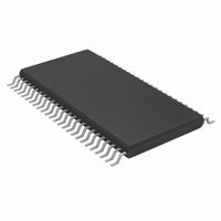
MAX9246EUM+TD Maxim Integrated Products, MAX9246EUM+TD Datasheet - Page 2

MAX9246EUM+TD
Manufacturer Part Number
MAX9246EUM+TD
Description
IC 21BIT DESERIALIZER 48-TSSOP
Manufacturer
Maxim Integrated Products
Datasheet
1.MAX9244EUMD.pdf
(23 pages)
Specifications of MAX9246EUM+TD
Function
Deserializer
Data Rate
306Mbps
Input Type
LVDS
Output Type
LVTTL, LVCMOS
Number Of Inputs
3
Number Of Outputs
21
Voltage - Supply
3 V ~ 3.6 V
Operating Temperature
-40°C ~ 85°C
Mounting Type
Surface Mount
Package / Case
48-TSSOP
Lead Free Status / RoHS Status
Lead free / RoHS Compliant
ABSOLUTE MAXIMUM RATINGS
(All voltages referenced to GND.)
V
V
RxIN__, RxCLKIN_.................................................-0.5V to +4.0V
PWRDWN ..............................................................-0.5V to +6.0V
SSG, DCB...................................................-0.5V to (V
RxOUT_, RxCLKOUT ...............................-0.5V to (V
Continuous Power Dissipation (T
ESD Protection
21-Bit Deserializers with Programmable
Spread Spectrum and DC Balance
Stresses beyond those listed under “Absolute Maximum Ratings” may cause permanent damage to the device. These are stress ratings only, and functional
operation of the device at these or any other conditions beyond those indicated in the operational sections of the specifications is not implied. Exposure to
absolute maximum rating conditions for extended periods may affect device reliability.
DC ELECTRICAL CHARACTERISTICS
(V
low, differential input voltage |V
noted. Typical values are at V
2
POWER SUPPLY
Power-Supply Range
Output-Supply Range
Worst-Case Supply Current
Human Body Model (R
CC
CCO
CC
48-Pin TSSOP (derate 16mW/°C above +70°C) ........1282mW
All Pins to GND .............................................................±2.5kV
, LVDSV
_______________________________________________________________________________________
......................................................................-0.5V to +6.0V
= LVDSV
PARAMETER
CC
CC
, PLLV
= PLLV
CC
D
.......................................-0.5V to +4.0V
CC
= 1.5kΩ, C
= +3.0V to +3.6V, V
CC
ID
A
= V
| = 0.05V to 1.2V, input common-mode voltage V
= +70°C)
LVDSV
SYMBOL
CCO
S
PLLV
V
I
= 100pF)
V
CCW
CCO
CC
= LVDSV
CC
,
CC
,
C
worst-case pattern,
V
to 3.6V, Figure 2
(MAX9242,
MAX9244,
MAX9254)
CCO
CC
L
CC
CCO
= 8pF,
CC
= V
= PLLV
= +3.0V to +5.5V, PWRDWN = high; SSG = high, open, or low; DCB = high or
+ 0.5V)
+ 0.5V)
CCO
CC
= 3.0V
= +3.3V, |V
CONDITIONS
Operating Temperature Range .........................-40°C to +105°C
Storage Temperature Range .............................-65°C to +150°C
Junction Temperature ......................................................+150°C
Lead Temperature (soldering, 10s) .................................+300°C
DC-balanced
mode (SSG = low)
Non-DC-balanced
mode (SSG = low)
D C - b al anced m od e
( S SG = hi g h or op en) 34MHz
N on- D C -b al anced
m ode
( S SG = hi g h or op en) 40MHz
IEC 61000-4-2 (R
ISO 10605 (R
LVDS Inputs to GND (Air-Gap Discharge).....................±15kV
LVDS Inputs to GND (Contact Discharge).......................±8kV
LVDS Inputs to GND (Air-Gap Discharge).....................±30kV
LVDS Inputs to GND (Contact Discharge).......................±6kV
ID
| = 0.2V, V
CM
D
= 2.0kΩ, C
= |V
D
CM
= 330Ω, C
16MHz
34MHz
20MHz
33MHz
40MHz
16MHz
20MHz
33MHz
ID
= +1.25V, T
/ 2| to 2.4V - |V
S
= 330pF)
S
MIN
= 150pF)
3.0
1.8
A
= +25°C.) (Notes 1, 2)
ID
TYP
101
107
50
81
55
75
83
62
67
93
/ 2|, unless otherwise
MAX
108
110
135
123
134
3.6
5.5
68
73
97
85
91
UNITS
mA
V
V


