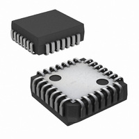
CLC020BCQ/NOPB National Semiconductor, CLC020BCQ/NOPB Datasheet - Page 11

CLC020BCQ/NOPB
Manufacturer Part Number
CLC020BCQ/NOPB
Description
IC SERIALIZER VIDEO DGTL 28-PLCC
Manufacturer
National Semiconductor
Datasheet
1.CLC020BCQNOPB.pdf
(15 pages)
Specifications of CLC020BCQ/NOPB
Function
Serializer
Data Rate
400Mbps
Input Type
CMOS
Output Type
CMOS, TTL
Number Of Inputs
10
Number Of Outputs
1
Voltage - Supply
4.5 V ~ 5.5 V
Operating Temperature
0°C ~ 70°C
Mounting Type
Surface Mount
Package / Case
28-PLCC
For Use With
SD020EVK - BOARD EVALUATION CLC020
Lead Free Status / RoHS Status
Lead free / RoHS Compliant
Other names
*CLC020BCQ
*CLC020BCQ/NOPB
CLC020BCQ
*CLC020BCQ/NOPB
CLC020BCQ
Available stocks
Company
Part Number
Manufacturer
Quantity
Price
Company:
Part Number:
CLC020BCQ/NOPB
Manufacturer:
National Semiconductor
Quantity:
135
Company:
Part Number:
CLC020BCQ/NOPB
Manufacturer:
LT
Quantity:
4 067
Company:
Part Number:
CLC020BCQ/NOPB
Manufacturer:
Texas Instruments
Quantity:
10 000
Application Information
Connect LOCK DETECT to TPG ENABLE for test pattern generator function.
Remove RP1 & RP3 and replace RP2 & RP4 with 50Ω resistor packs for coax interfacing.
Install RP1-4 when using ribbon cable for input interfacing.
This board is designed for use with TTL power supplies only.
For optional ECL compatible load: R1A = R2A = 187; R1B = R2B = 124.
All resistances & impedances in Ohms. Values with 3 significant digits are 1%; with 2 digits 5%.
MEASURING JITTER
The test method used to obtain the timing jitter value given in
the AC Electrical Specification table is based on procedures
and equipment described in SMPTE RP 192-1996. The rec-
ommended practice discusses several methods and indica-
tor devices. An FFT method performed by standard video
test equipment was used to obtain the data given in this data
sheet. As such, the jitter characteristics (or jitter floor) of the
measurement equipment, particularly the measurement ana-
lyzer, become integral to the resulting jitter value. The
method and equipment were chosen so that the test can be
easily duplicated by the design engineer using most stan-
dard digital video test equipment. In so doing, similar results
should be achieved. The intrinsic jitter floor of the CLC020’s
PLL is approximately 25% of the typical jitter given in the
electrical specifications. In production, device jitter is mea-
sured on automatic IC test equipment (ATE) using a different
method compatible with that equipment. Jitter measured
using this ATE yields values approximately 50% of those
obtained using the video test equipment.
FIGURE 8. SD020EVK Schematic Diagram
(Continued)
11
The jitter test setup used to obtain values quoted in the data
sheet consists of:
Apply the black-burst reference clock from the TG2000 sig-
nal generator’s BG1 module 27MHz clock output to the level
converter input. The clock amplitude converter schematic is
shown in Figure 9. Adjust the input bias control to give a 50%
duty cycle output as measured on the oscilloscope/probe
system. Connect the level translator to the SD020EVK
board, connector P1, P
• National Semiconductor SD020EVK, CLC020 evaluation
• Tektronix TG2000 signal generation platform with DVG1
• Tektronix VM700T Option 1S Video Measurement Set
• Tektronix TDS 794D, Option C2 oscilloscope
• Tektronix P6339A passive probe
• 75 Ohm coaxial cable, 3ft., Belden 8281 or RG59 (2
• ECL-to-TTL/CMOS level converter/amplifier, Figure 10
kit
option
required)
CLK
pins (the outer-most row of pins
www.national.com
10091709


